

Magneto-resistor element with three-decker memory layer
A technology of magnetoresistance and memory layer, applied in the field of vertical magnetoresistance elements, can solve the problems of poor thermal stability and unsolved MR rate, and achieves reduction of damping coefficient, increase of current spin polarizability, and high MR rate. Effect
- Summary
- Abstract
- Description
- Claims
- Application Information
AI Technical Summary
Problems solved by technology
Method used
Image

Examples
Embodiment 1
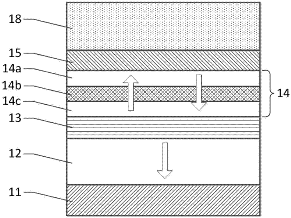
[0038] figure 1 It is a structural schematic diagram of an MTJ element based on the present invention, which includes a bottom electrode 11, a reference layer 12, a barrier layer 13, a memory layer 14, a lattice optimization layer 15 and a base layer 18 arranged adjacently in sequence from bottom to top, wherein The memory layer 14 is composed of a first memory sublayer 14a, a second memory sublayer 14c, and an insertion layer 14b between the first memory sublayer 14a and the second memory sublayer 14c, which are sequentially adjacent.
[0039] The reference layer 12 is a ferromagnetic material, the magnetization direction of the reference layer 12 is constant and the magnetic anisotropy is perpendicular to the layer surface; in the memory layer 14, the first memory sublayer 14a and the second memory sublayer 14c are ferromagnetic materials, The insertion layer 14b is a non-magnetic material, and the magnetization direction of the memory layer 14 as a whole is variable and the...
Embodiment 2
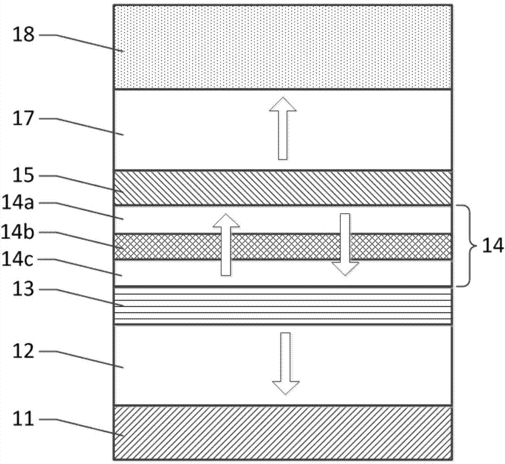
[0051] figure 2 is in figure 1 A schematic diagram of the structure of an MTJ element further improved on the basis of the device structure in the medium, including a bottom electrode 11, a reference layer 12, a barrier layer 13, a memory layer 14, a lattice optimization layer 15, and a magnetic correction Layer 17 and base layer 18, wherein the memory layer 14 consists of successively adjacent first memory sublayer 14a, second memory sublayer 14c, and an insert layer between the first memory sublayer 14a and the second memory sublayer 14c 14b composition. and figure 1 The difference in device structure is that a magnetic correction layer 17 is added between the lattice optimization layer 15 and the base layer 18 .
[0052] The characteristics of the magnetic correction layer 17 are similar to those of the reference layer 12, in that the magnetization direction is constant and the magnetic anisotropy is perpendicular to the layer surface; the magnetization direction of the...
Embodiment 3
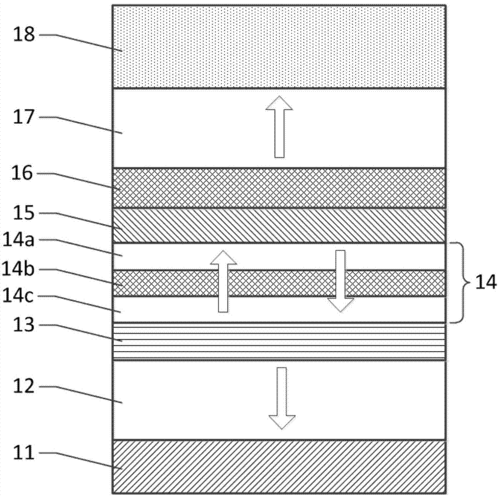
[0056] image 3 is in figure 2 A schematic diagram of the structure of an MTJ element further improved on the basis of the device structure in the medium, including a bottom electrode 11, a reference layer 12, a barrier layer 13, a memory layer 14, a lattice optimization layer 15, a spin Polarization stabilization layer 16, magnetic correction layer 17 and foundation layer 18, wherein memory layer 14 is made up of successively adjacent first memory sublayer 14a, second memory sublayer 14c and between first memory sublayer 14a and second memory Inserted layer 14b between sub-layers 14c. and figure 2 The difference in device structure is that a spin polarization stabilization layer 16 is added between the magnetic correction layer 17 and the lattice optimization layer 15 .
[0057] The spin polarization stable layer 16 has higher electron polarization conductivity, and the electron spin polarization loss rate on the Fermi level is close to zero, and the spin polarization st...
PUM
| Property | Measurement | Unit |
|---|---|---|
| Thickness | aaaaa | aaaaa |
| Thickness | aaaaa | aaaaa |
| Thickness | aaaaa | aaaaa |
Abstract
Description
Claims
Application Information