Production method for HDI plate

A production method and integrated technology, applied in the direction of multi-layer circuit manufacturing, printed circuit manufacturing, and the formation of electrical connection of printed components, can solve the problems of short process flow, long process flow, worn out boards, etc., and achieve a short production process and reduce The effect of over-etching and improving product yield

Inactive Publication Date: 2015-07-08
SHENZHEN SUNTAK MULTILAYER PCB
View PDF6 Cites 1 Cited by
  • Summary
  • Abstract
  • Description
  • Claims
  • Application Information

AI Technical Summary

Problems solved by technology

[0003] The present invention aims at the problems of making thin HDI boards in the prior art, which are prone to curling, jamming, deformation and wear, and long process flow, etc., and provides a production of HDI boards with short process flow, high yield rate and guaranteed quality method

Method used


Image

  • Production method for HDI plate

Examples


Embodiment

[0014] This embodiment provides a method for manufacturing an HDI board (with a finished thickness of 0.5mm), and the specific manufacturing steps are as follows:

[0015] (1) According to the circuit board production process of the prior art, the circuit board raw material is cut to obtain the substrate, and then the inner layer pattern transfer and etching are performed on the substrate to form the inner layer circuit on the substrate to obtain the inner layer core board. After the inner layer core board is pre-pressed, the inner layer core board and the copper foil are pressed together through the prepreg to form a multi-layer inner layer board.

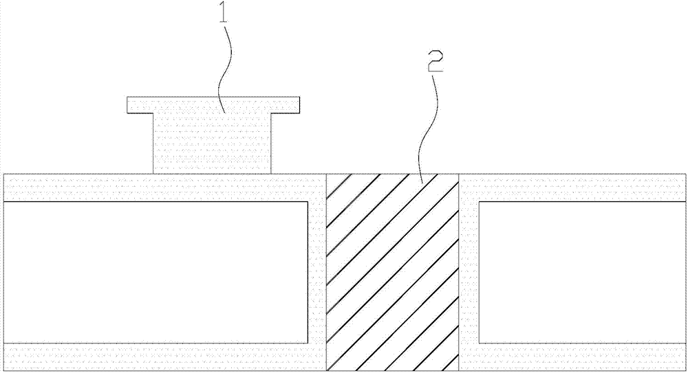
[0016] Then, according to the existing technology of laser drilling blind holes and mechanical drilling through holes, the required blind holes and / or through holes are drilled at the positions where blind holes and / or through holes need to be made on the multilayer inner layer board, that is, drilling out the required slot.

[0...


PUM

PropertyMeasurementUnit
thicknessaaaaaaaaaa

Abstract

The invention relates to the technical field of circuit board production, in particular to a production method for an HDI plate. According to the production method for the HDI plate, the HDI plate with thickness ranging from 0.3 mm to 0.7 mm is produced, a prepreg fills a metallized slotted hole produced in the step 1 during pressuring, and at the same time a metallized blind hole and/or a metallized through hole produced in the step 2 and the metallized slotted hole produced in the step 1 are staggered, so that the processes of resin hole plugging and abrasive belt plate grinding are reduced, producing a cooper cap above the metallized slotted groove is not needed, and the production procedures are reduced greatly. According to the production method for the HDI plate, the abrasive belt plate grinding is not needed to be conducted, the occurrence of the problems of plate rolling, plate clamping, deforming and plate wearing and the like can be avoided, and the product yield is improved; due to the fact that producing the cooper cap above the metallized slotted groove is not needed, the uniformity of a copper layer can be improved, conducting etching is facilitated, and the occurrence of the problems of excessive etching or under etching is reduced. The production method for the HDI plate is short in production processes, and lowering cost and controlling quality risk are facilitated.

Description

technical field [0001] The invention relates to the technical field of circuit board manufacturing, in particular to a method for manufacturing an HDI board. Background technique [0002] HDI is the English abbreviation of High Density Interconnector. HDI boards are commonly referred to as high-density circuit boards. High-density interconnect (HDI) manufacturing is one of the fastest-growing fields in the printed circuit board industry. With the development needs of electronic products, the design and application of HDI boards are becoming more and more extensive. Using the existing technology to manufacture HDI boards requires a resin plugging process, and for the resin plugging process, it is necessary to introduce the abrasive belt grinding process accordingly, and it is also necessary to make a copper cap (CAP-Copper) above the resin plugging hole. ) as the bottom PAD of laser drilling to prevent laser drilling breakdown. However, if the existing technology is used to...

Claims


Application Information

Patent Timeline
Patent Type & Authority Applications(China)
IPC IPC(8): H05K3/42H05K3/46
CPCH05K3/429H05K3/4652
Inventor 张国城张军杰韩启龙刘东
Owner SHENZHEN SUNTAK MULTILAYER PCB
Why Eureka
Try Eureka