Method and device for growing high-purity semi-insulating silicon carbide single crystal

A silicon carbide single crystal, semi-insulating technology, applied in chemical instruments and methods, single crystal growth, single crystal growth, etc., can solve the problems of low solubility, high difficulty, reduced N content, high-purity semi-insulating SiC, etc.

Active Publication Date: 2015-07-15
SICC CO LTD
View PDF6 Cites 17 Cited by
  • Summary
  • Abstract
  • Description
  • Claims
  • Application Information

AI Technical Summary

Problems solved by technology

However, vanadium-doped SiC also has some problems: the solubility of vanadium in SiC is very low, and it is easy to form precipitates, which will lead to the formation of defects such as micropipes, which seriously affects the crystal quality. More importantly, the vanadium-doped SiC substrate Deep trapping centers affect the power output of high-frequency high-power devices, so the preparation of high-purity semi-insulating SiC single crystals has become a current research hotspot
[0004] The key to high-purity semi-insulating SiC single crystal growth technology is to remove the two impurities B and N in the crystal. B is an impurity that coexists with graphite, and graphite crucibles, insulation materials, and SiC source materials will all adsorb N. Therefore, removing these...

Method used


Image

  • Method and device for growing high-purity semi-insulating silicon carbide single crystal
  • Method and device for growing high-purity semi-insulating silicon carbide single crystal
  • Method and device for growing high-purity semi-insulating silicon carbide single crystal

Examples


Embodiment 1

[0043] A method for growing a high-purity semi-insulating SiC single crystal, realized by the following device for growing a high-purity semi-insulating silicon carbide single crystal;

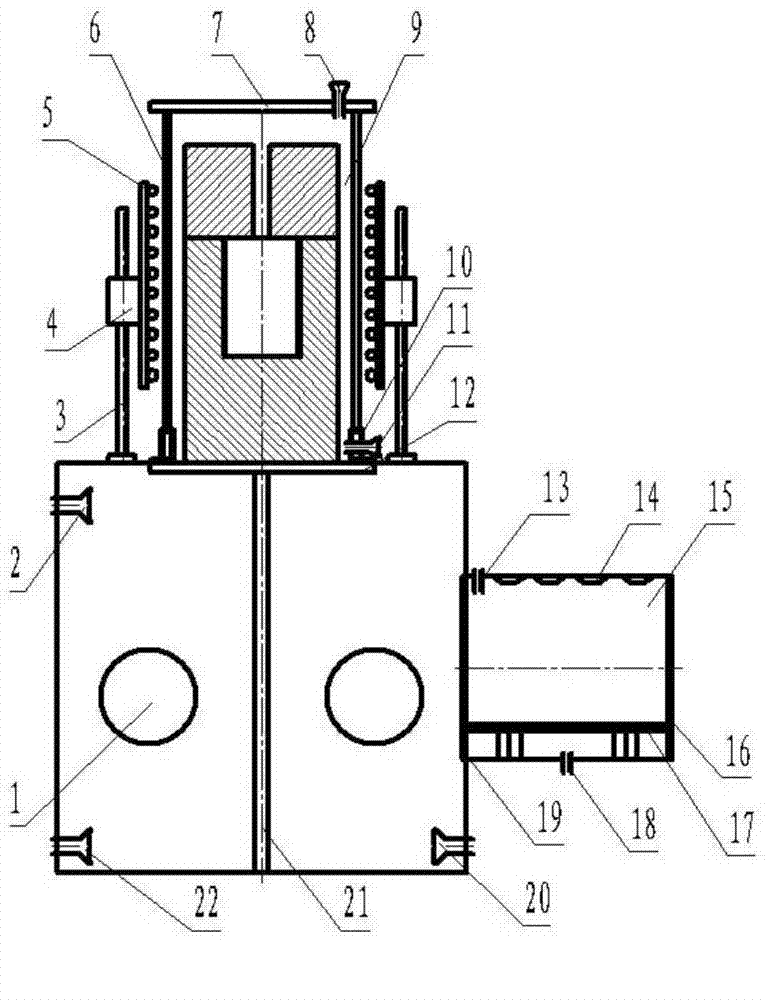
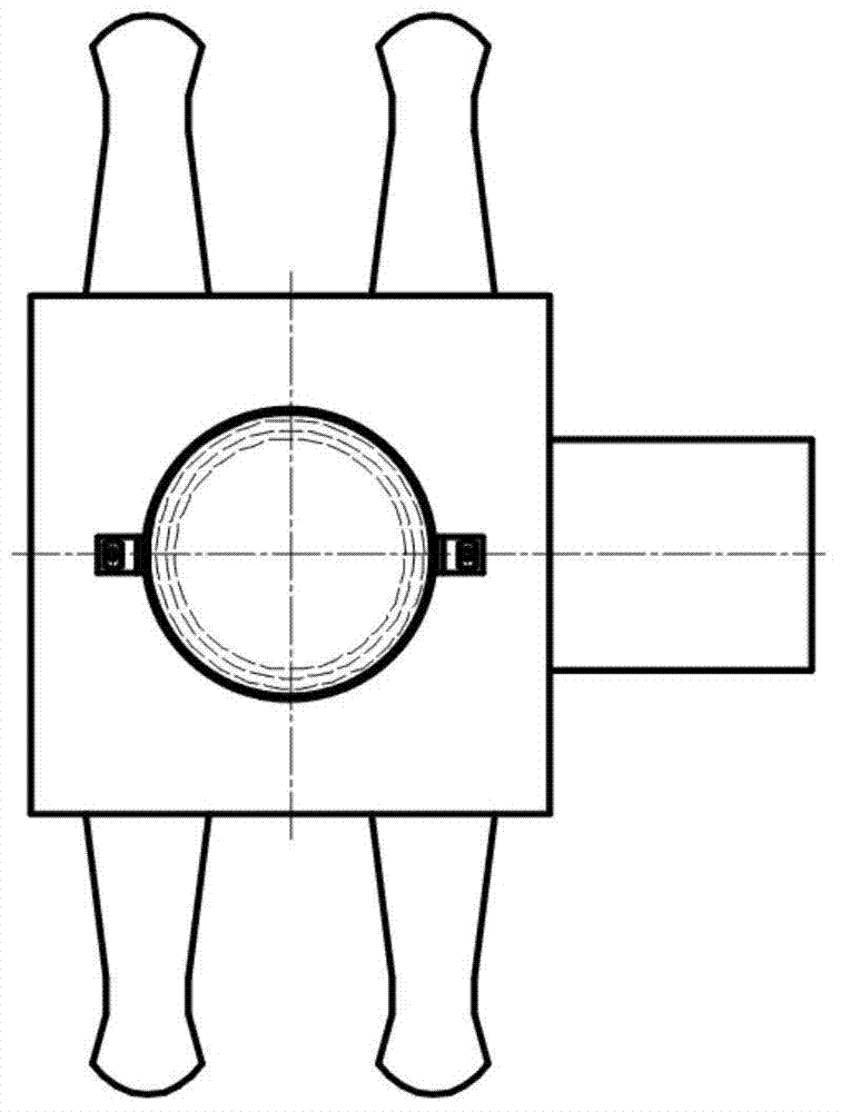
[0044] The device comprises a growth chamber, the growth chamber adopts a lower opening method, an induction heater is arranged outside the growth chamber, an atmospheric isolation chamber is connected to the lower part of the growth chamber, an operation window is arranged on the atmospheric isolation chamber, and the atmospheric isolation chamber One side is connected with a transition chamber, the transition chamber is equipped with a heating device for removing impurities, the atmosphere isolation chamber and the transition chamber are equipped with a mechanism to keep the internal environment in a protective gas state or a vacuum state, and the lower part of the atmosphere isolation chamber is also Equipped with a vacuum cleaner interface;

[0045] Both the atmospheric isolation chamber a...

Embodiment 2

[0051] A method for growing a high-purity semi-insulating silicon carbide single crystal, realized by the following device for growing a high-purity semi-insulating SiC single crystal;

[0052] The device comprises a growth chamber, the growth chamber adopts a lower opening method, an induction heater is arranged outside the growth chamber, an atmospheric isolation chamber is connected to the lower part of the growth chamber, an operation window is arranged on the atmospheric isolation chamber, and the atmospheric isolation chamber One side is connected with a transition chamber, the transition chamber is equipped with a heating device for removing impurities, the atmosphere isolation chamber and the transition chamber are equipped with a mechanism to keep the internal environment in a protective gas state or a vacuum state, and the lower part of the atmosphere isolation chamber is also Equipped with a vacuum cleaner interface;

[0053] Both the atmospheric isolation chamber a...

Embodiment 3

[0061] A method for growing a high-purity semi-insulating silicon carbide single crystal, realized by the following device for growing a high-purity semi-insulating SiC single crystal;

[0062] The device comprises a growth chamber, the growth chamber adopts a lower opening method, an induction heater is arranged outside the growth chamber, an atmospheric isolation chamber is connected to the lower part of the growth chamber, an operation window is arranged on the atmospheric isolation chamber, and the atmospheric isolation chamber One side is connected with a transition chamber, the transition chamber is equipped with a heating device for removing impurities, the atmosphere isolation chamber and the transition chamber are equipped with a mechanism to keep the internal environment in a protective gas state or a vacuum state, and the lower part of the atmosphere isolation chamber is also Equipped with a vacuum cleaner interface;

[0063] Both the atmospheric isolation chamber a...


PUM

PropertyMeasurementUnit
Resistivityaaaaaaaaaa

Abstract

The invention relates to a method and device for growing a high-purity semi-insulating silicon carbide single crystal and belongs to the technical field of single crystal growth. A crucible and thermal insulation materials for growing a SiC single crystal are pre-processed by utilizing a specific device, specific gas is introduced in the single crystal growth process, the donor impurities N, acceptor impurities B and metal ions impurities in the SiC single crystal are effectively reduced, the specific resistance is enhanced, the power output of high-frequency and high-power devices is prevented from being affected by the deep capture center of vanadium-doped semi-insulating SiC, and the high-purity semi-insulating silicon carbide single crystal is obtained.

Description

technical field [0001] The invention relates to a method and device for growing a high-purity semi-insulating silicon carbide single crystal, belonging to the technical field of single crystal growth. Background technique [0002] The semi-insulating SiC single crystal polished wafer is the best substrate for the preparation of wide-bandgap solid-state microwave devices at this stage, and it also plays a very important role in power devices and deep submicron devices. More importantly, in terms of electrical properties and thermal conductivity, semi-insulating SiC is a new generation of wide-bandgap semiconductor materials that have great application prospects in optoelectronic and microwave power devices. [0003] Researchers usually introduce deep-level impurity vanadium into SiC crystals to form deep compensation levels, which are located near the center of the forbidden band and can well bind carriers. Currently only vanadium-doped SiC exhibits high-resistance propertie...

Claims


Application Information

Patent Timeline
IPC IPC(8): C30B13/20C30B29/36
Inventor 高玉强宗艳民宋建王希杰张红岩
Owner SICC CO LTD
Why Eureka
Try Eureka