Detection device and method for thin-film transistor array substrate

A technology of thin-film transistors and array substrates, which is applied in the field of detection devices for thin-film transistor array substrates, can solve problems such as missed inspections of products, and achieve the effects of avoiding missed inspections and enhancing electrical activity

Active Publication Date: 2015-07-22
KUSN INFOVISION OPTOELECTRONICS
View PDF8 Cites 4 Cited by
  • Summary
  • Abstract
  • Description
  • Claims
  • Application Information

AI Technical Summary

Problems solved by technology

Because the amorphous silicon residue 109 is a semiconductor, there are not too many carriers (a lot less than the free electrons in the conductor), the amorphous silicon residue 109 has little change in the voltage on the data line 102, and the amorphous silicon residue 109 cannot be connected with the pixel. The electrode 25 acts directly, and can only change the pixel voltage through the capacitive coupling effect, which has little influence on the pixel voltage. Therefore, it is difficult to detect the amorphous silicon residue 109 during the above detection process, which may easily lead to leakage of defective products. check

Method used


Image

  • Detection device and method for thin-film transistor array substrate
  • Detection device and method for thin-film transistor array substrate
  • Detection device and method for thin-film transistor array substrate

Examples


Embodiment Construction

[0027] In order to further illustrate the technical means and functions adopted by the present invention to achieve the intended invention purpose, the present invention will be described in detail below in conjunction with the accompanying drawings and preferred embodiments.

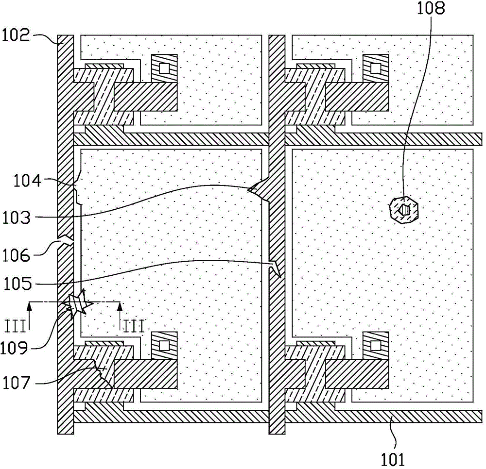
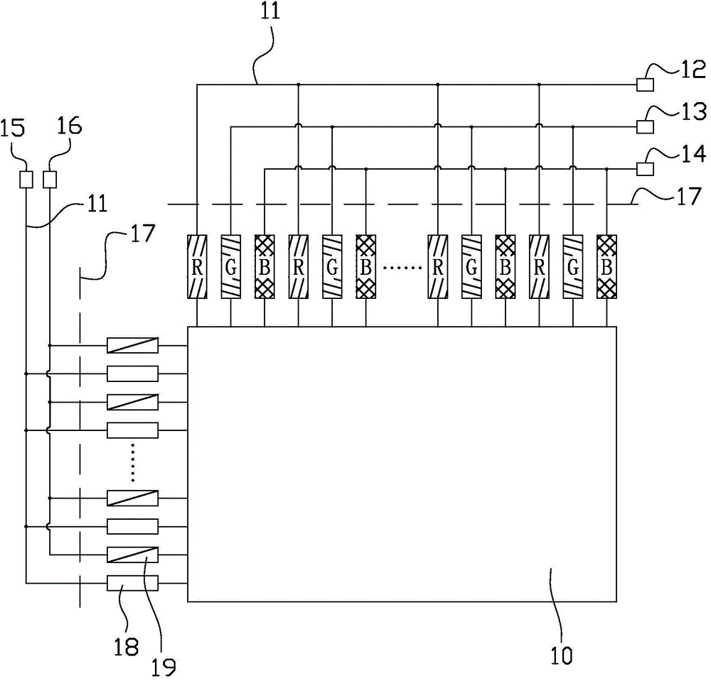
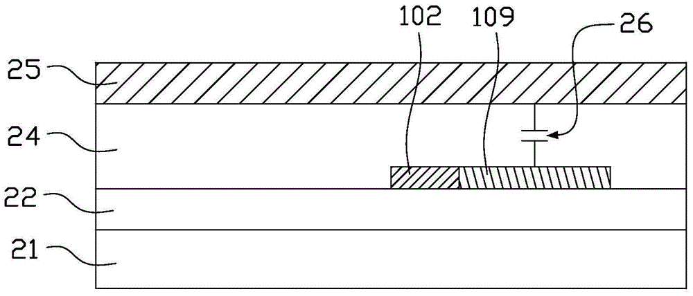
[0028] An embodiment of the present invention provides a detection device (array tester) for a thin film transistor array substrate, which is used for detecting whether there is a pixel defect in the manufactured thin film transistor array substrate, especially for detecting whether there is amorphous silicon (a-Si ) remains.

[0029] The electrical properties of amorphous silicon semiconductors change strongly with temperature, that is, the higher the temperature, the stronger the electrical properties. This change is mainly due to the change of carrier concentration in the semiconductor with temperature. For an absolutely pure semiconductor at absolute zero, the semiconductor covalent bond is saturate...


PUM


Abstract

The invention provides a detection device of a thin-film transistor array substrate and used for conducting the defect detecting on the thin-film transistor array substrate. The detection device comprises a carrying table base and a heating device arranged on the carrying table base, wherein the heating device is used for heating the thin-film transistor array substrate placed on the carrying table base before the defect detecting is conducted. The invention further provides a detection method for the thin-film transistor array substrate. By utilization of the thermo-sensitive properties, the thin-film transistor array substrate to be detected is heated and warmed through the arrangement of the heating device, the detection method can increase the number of the current carrier in the amorphous silicon residue of the thin-film transistor array substrate, increases the electrical activity of the amorphous silicon residue, enhances the influence of the amorphous silicon residue on the pixel voltage during detection, is beneficial for the pixel defect detection of the amorphous silicon residue, and avoids the leak detection of the defected products.

Description

technical field [0001] The invention relates to the technical field of liquid crystal display, in particular to a detection device and a detection method of a thin film transistor array substrate. Background technique [0002] In the manufacturing process of the liquid crystal panel, it is first necessary to use a glass substrate as a substrate, and fabricate a thin film transistor (Thin Film Transistor, TFT) array on the glass substrate, so as to fabricate a thin film transistor array substrate. When making a TFT array, it is necessary to use multiple photomask processes to separately fabricate each layer structure of the TFT, such as the gate layer, gate insulating layer, semiconductor layer, source and drain layers, passivation protection layer, etc., each photomask process For example, it includes process steps such as film deposition, photoresist application, exposure and development, etching, and photoresist stripping. [0003] figure 1 It is a plan view of a partial...

Claims


Application Information

Patent Timeline
Patent Type & Authority Applications(China)
IPC IPC(8): H01L21/66G02F1/13
CPCG02F1/13H01L22/30
Inventor 吴金力沈磊
Owner KUSN INFOVISION OPTOELECTRONICS
Why Eureka
Try Eureka