A kind of preparation method of LED photonic crystal

A technology of photonic crystals and light beams, applied in semiconductor devices, electrical components, circuits, etc., can solve the problems of difficult photonic crystal nanoprocessing technology, unfavorable large-scale production, complex process steps, etc., to achieve increased luminous power, low processing, and The effect of simple process

Inactive Publication Date: 2017-10-03
DALIAN NATIONALITIES UNIVERSITY
View PDF3 Cites 0 Cited by
  • Summary
  • Abstract
  • Description
  • Claims
  • Application Information

AI Technical Summary

Problems solved by technology

[0003] The present invention provides a method for preparing LED photonic crystals in order to solve the problems in the prior art that the preparation of photonic crystal nano-processing technology is difficult, the process steps are complicated, the cost is high, and it is not conducive to large-scale production.

Method used


Image

  • A kind of preparation method of LED photonic crystal

Examples


Embodiment 1

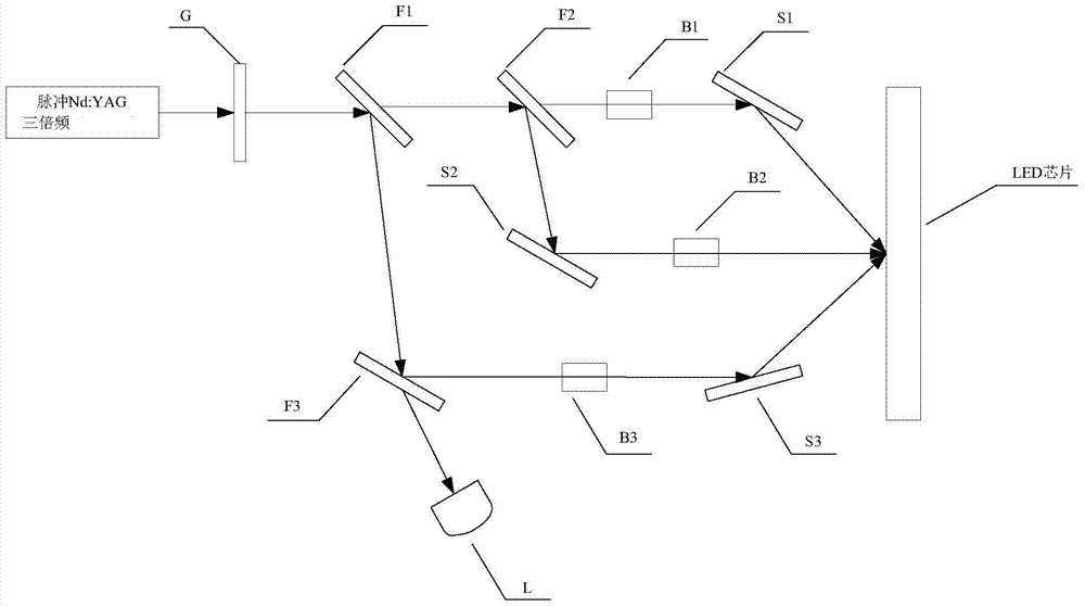
[0022] Such as figure 1 As shown, using the triple frequency laser beam (355nm) of Nd:YAG laser as the direct etching laser, on the GaN chip, photonic crystals with different periods and different depths of the triangular lattice were prepared on the ITO layer. After the frequency-doubled laser beam passes through the diaphragm G, it is divided into a first beam and a second beam through the first beam splitter F1; the first beam is divided into a third beam and a fourth beam through the second beam splitter F2; The second beam is divided into a fifth beam and a sixth beam by the third beam splitter F3; the sixth beam is directly input to the optical power meter L for detecting and monitoring the power of the Nd:YAG laser. The third light beam, the fourth light beam and the fifth light beam are respectively modulated by polarizers and reflectors and converged on the transparent electrode film of the LED chip at the same time, that is, the third light beam passes through the fi...

Embodiment 2

[0024] Such as figure 1 As shown, the frequency tripled laser beam of Nd:YAG laser is used as the direct etching laser, and on the GaN chip, photonic crystals with different periods and different depths of the triangular lattice are prepared on the ITO layer, and the frequency tripled laser After the beam passes through the aperture G, it is divided into a first beam and a second beam through the first beam splitter F1; the first beam is divided into a third beam and a fourth beam through the second beam splitter F2; the second beam is passed through The third beam splitter F3 is divided into a fifth light beam and a sixth light beam; the sixth light beam is directly input to the optical power meter L for detecting and monitoring the power of the Nd:YAG laser. The third light beam, the fourth light beam and the fifth light beam are respectively modulated by polarizers and reflectors and converged on the transparent electrode film of the LED chip at the same time, that is, the ...

Embodiment 3

[0025] Such as figure 1 As shown, the frequency tripled laser beam of Nd:YAG laser is used as the direct etching laser, and on the GaN chip, photonic crystals with different periods and different depths of the triangular lattice are prepared on the ITO layer, and the frequency tripled laser After the beam passes through the aperture G, it is divided into a first beam and a second beam through the first beam splitter F1; the first beam is divided into a third beam and a fourth beam through the second beam splitter F2; the second beam is passed through The third beam splitter F3 is divided into a fifth light beam and a sixth light beam; the sixth light beam is directly input to the optical power meter L for detecting and monitoring the power of the Nd:YAG laser. The third light beam, the fourth light beam and the fifth light beam are respectively modulated by polarizers and reflectors and converged on the transparent electrode film of the LED chip at the same time, that is, the ...


PUM


Abstract

The invention relates to a preparation method of an LED photonic crystal. The method comprises the steps of splitting a triple-frequency laser beam of Nd: YAG laser, which is used as direct etching laser and the wavelength of which is gamma, into three coherent laser beams, wherein every two coherent laser beams form an identical angle theta, each coherent laser beam is identical in polarization direction, and converging the three coherent laser beams onto a transparent electrode film of an LED chip; applying one or more pulses to the Nd: YAG laser, and finally forming the photonic crystal with a given period T and given porosity. By adopting the method, the photonic crystal can be prepared on the surface of the chip in one step, the process is simple, convenience and rapidness can be realized, and the steps such as masking and after-treatment are not needed; the prepared photonic crystal is controllable in period, and the photonic crystal with the period of 300nm to 300 micrometers can be obtained by changing the range of the angle theta; the processing area is large, the processing cost is low, and the method is applicable to batch and mass production.

Description

technical field [0001] The invention relates to the field of photonic crystals, and more specifically, to a preparation method of LED photonic crystals. Background technique [0002] Photonic crystals refer to artificial periodic dielectric structures with photonic band gap characteristics, and photonic crystals are one of the important ways to improve the light extraction efficiency of GaN-based blue LEDs. Theoretically, photonic crystals improve LED light extraction efficiency by utilizing the photonic crystal bandgap structure corresponding to the output light wavelength of the LED, and converting the guided wave mode confined in the light-emitting layer into a radiation mode. For an LED with a given output light wavelength, a photonic crystal with a specific lattice type and geometric structure is prepared on its surface. Generally, the photonic crystal with this structure is required to have a photonic band gap at the light wavelength (or frequency). Most of the existi...

Claims


Application Information

Patent Timeline
Patent Type & Authority Patents(China)
IPC IPC(8): H01L33/42H01L33/00
CPCH01L33/005H01L33/0095H01L33/02H01L33/42H01L2933/0016
Inventor 刘中凡王作斌
Owner DALIAN NATIONALITIES UNIVERSITY
Why Eureka
Try Eureka