Supercharge Your Innovation With Domain-Expert AI Agents!

Novel Wafer Bonding device

A new type of equipment technology, applied in electrical components, semiconductor/solid-state device manufacturing, circuits, etc., can solve the problems of large consumption of graphite materials, damaged blocks of graphite parts, and high equipment failure rate, achieving fast heating speed and easy maintenance. , the effect of long life

Inactive Publication Date: 2015-07-29
山西立强科技有限公司
View PDF7 Cites 1 Cited by
  • Summary
  • Abstract
  • Description
  • Claims
  • Application Information

AI Technical Summary

Problems solved by technology

[0005] The present invention overcomes the deficiencies in the prior art, solves the problems of low production efficiency, high equipment failure rate, damaged graphite parts, and large consumption of graphite materials in the existing Wafer Bonding process technology, and aims to provide a new Wafer Bonding Bonding process equipment

Method used


Image

  • Novel Wafer Bonding device
  • Novel Wafer Bonding device

Examples


Embodiment Construction

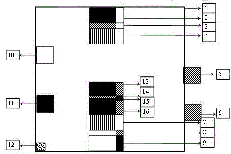
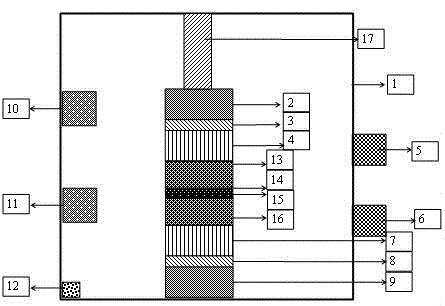
[0017] Such as figure 1 As shown, the new Wafer Bonding equipment includes a vacuum chamber 1. A vacuum generator 12 is arranged inside the vacuum chamber 1. An upper pressure control system and a lower pressure control system are respectively arranged on the upper and lower walls of the vacuum chamber 1. The pressure control system is movably connected with the front wall of the vacuum chamber 1 through the telescopic connection shaft 17, and the telescopic connection shaft 17 drives the upper pressure control system to rise and fall. The upper pressure control system consists of the upper pressure cylinder 2, the upper heat insulation The layer 3 and the upper heater 4 are composed, and the lower pressure control system is composed of the lower pressure cylinder 9, the lower heat insulation layer 8 and the lower heater 7.

[0018] The outer wall of the vacuum chamber 1 is provided with an upper microwave generator 5 and a lower microwave generator 6 in sequence, and the uppe...


PUM


Abstract

The invention discloses a novel Wafer Bonding device, belongs to the field of wafer welding devices and solves the problems of low production efficiency, high failure rate, rapid graphite accessory damage, high graphite material consumption and the like of existing Wafer Bonding process technology. The novel Wafer Bonding device comprises a vacuum cavity, an upper pressure control system and a lower pressure control system are arranged on the inner upper wall and the inner lower wall of the vacuum cavity respectively, the upper pressure control system is movably connected with the front wall of the vacuum cavity through a telescopic connecting shaft, the telescopic connecting shaft drives the upper pressure control system to rise and fall, an upper microwave generator and a lower microwave generator are sequentially arranged on the outer side wall of the vacuum cavity and correspondingly irradiate an upper heater and a lower heater respectively, and an upper temperature detector and a lower temperature detector are sequentially arranged on the inner side wall of the vacuum cavity, monitor the temperatures of the upper heater and the lower heater in real time and are connected with the upper microwave generator and the lower microwave generator to form a feedback adjusting system.

Description

technical field [0001] The novel Wafer Bonding equipment of the invention belongs to the field of wafer welding equipment. Background technique [0002] At present, in order to improve the light output efficiency and heat dissipation performance of the LED chip production process, a large number of LED chip substrates are replaced by the Wafer Bonding process. The substrate is a metal substrate with good thermal conductivity, electrical conductivity and high light reflection efficiency, or a silicon substrate. substrate. [0003] In the traditional Wafer Bonding process, graphite heaters are used to heat and graphite fixtures are used as temperature conductors to heat and press the bonding materials. The heating rate and cooling rate are slow, and the life of the graphite heater is short and the failure rate is high, resulting in Wafer The cost of bonding process is rising rapidly. [0004] Microwaves have great penetrating ability. When heating, heat can be generated dire...

Claims


Application Information

Patent Timeline
IPC IPC(8): H01L21/60
CPCH01L21/67126
Inventor 李少辉
Owner 山西立强科技有限公司
Features
  • R&D
  • Intellectual Property
  • Life Sciences
  • Materials
  • Tech Scout
  • Unparalleled Data Quality
  • Higher Quality Content
  • 60% Fewer Hallucinations
Learn More