Thin-film transistor and liquid crystal displayer

一种薄膜晶体管、基板的技术,应用在电固体器件、半导体器件、半导体/固态器件零部件等方向,能够解决薄膜晶体管电性能不利影响、易受到外界因素的影响、氧化物电性能不够稳定等问题,达到良好显示品质、避免不利影响、良好性能的效果

Active Publication Date: 2015-07-29
TCL CHINA STAR OPTOELECTRONICS TECH CO LTD +1
View PDF6 Cites 3 Cited by
  • Summary
  • Abstract
  • Description
  • Claims
  • Application Information

AI Technical Summary

Problems solved by technology

However, the electrical properties of these oxides are not stable enough and are easily affected by external factors, especially light
For example, light exposure can affect the electrical properties of these oxides, resulting in increased leakage current, which can adversely affect the electrical properties of thin film transistors

Method used


Image

  • Thin-film transistor and liquid crystal displayer
  • Thin-film transistor and liquid crystal displayer
  • Thin-film transistor and liquid crystal displayer

Examples


Embodiment Construction

[0022] The present invention will be further described below in conjunction with accompanying drawing.

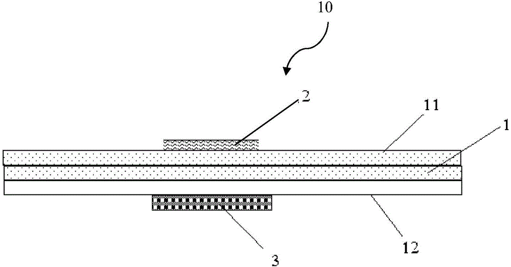
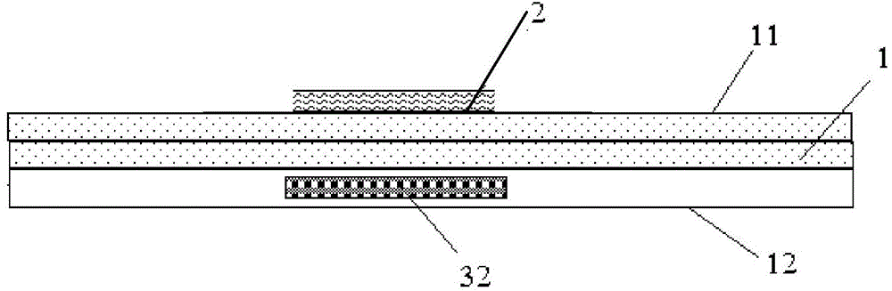
[0023] figure 1 A first embodiment of a thin film transistor 10 according to the invention is schematically shown. Such as figure 1 As shown, a thin film transistor 10 includes a substrate 1 , a conductive layer 2 disposed on the substrate 1 , and a light shielding layer 3 disposed on the substrate 1 . The substrate 1 can be a transparent glass substrate. The conductive stack 2 generally includes a source, a drain, an oxide active layer, a gate insulating layer and a gate, which are well known to those skilled in the art and will not be repeated here. The light shielding layer 3 is an opaque layer.

[0024] The light-shielding layer 3 is under the conductive stack 2 and the position of the light-shielding layer 3 is directly opposite to the position of the conductive stack 2 . In this way, the light 5 from below the substrate 1 will not irradiate the conductive stack 2...


PUM


Abstract

The invention relates to a thin-film transistor and a liquid crystal displayer. The thin-film transistor comprises a substrate, a conductive lamination layer which is arranged on the substrate, and a light shielding layer which is arranged on the substrate. The light shielding layer is arranged below the conductive lamination layer, and the positions of the light shielding layer and the conductive lamination layer are exactly opposite. The thin-film transistor is provided with the light shielding layer used for light shielding of the conductive lamination layer so that adverse influence of illumination on electrical properties of oxides can be effectively prevented, and thus the electrical properties of the thin-film transistor can be enhanced.

Description

technical field [0001] The invention relates to the field of liquid crystal display, in particular to a thin film transistor. The invention also relates to a liquid crystal display comprising such a thin film transistor. Background technique [0002] Currently, in liquid crystal displays, thin film transistors (ie, TFTs well known to those skilled in the art) are widely used to drive each liquid crystal pixel on the liquid crystal display. Therefore, the electrical performance of the thin film transistor has an important relationship with the quality of the liquid crystal display. [0003] Typically, thin film transistors are stacked from multiple layers of oxides (ie conductive stacks). However, the electrical properties of these oxides are not stable enough and are very susceptible to external factors, especially light. For example, light will affect the electrical properties of these oxides, resulting in increased leakage current, which will adversely affect the electr...

Claims


Application Information

Patent Timeline
Patent Type & Authority Applications(China)
IPC IPC(8): H01L29/768G02F1/1343H01L27/12G02F1/1335
CPCG02F1/133512G02F1/1343G02F1/1362H01L23/552H01L27/1214H01L29/768G02F1/136209G02F1/1368H01L27/1218H01L29/78633H01L27/1225H01L29/7869
Inventor 卢廷豪
Owner TCL CHINA STAR OPTOELECTRONICS TECH CO LTD
Why Eureka
Try Eureka