GaN-based light-emitting diode epitaxial wafer production method and produced epitaxial wafer

A technology of light-emitting diodes and epitaxial wafers, which is applied in the direction of electrical components, circuits, semiconductor devices, etc., can solve the problems of large stress in multi-quantum well layers, reduce luminous efficiency, and lattice mismatch, so as to reduce the polarization electric field and improve the growth rate. quality, slow down the effect of continuing to extend

Active Publication Date: 2015-07-29
HC SEMITEK SUZHOU
View PDF6 Cites 26 Cited by
  • Summary
  • Abstract
  • Description
  • Claims
  • Application Information

AI Technical Summary

Problems solved by technology

[0006] Embodiments of the present invention provide a GaN-based light-emitting diode epitaxial wafer preparation method and the prepared epitaxial wafer, which can solve the problems caused by the lattice mismatch and thermal expansion coefficient difference between the substrate and the epitaxial layer. Larger stress, which in turn causes the piezoelectric polarization effect, which reduces the luminous efficiency of the LED

Method used


Image

  • GaN-based light-emitting diode epitaxial wafer production method and produced epitaxial wafer
  • GaN-based light-emitting diode epitaxial wafer production method and produced epitaxial wafer
  • GaN-based light-emitting diode epitaxial wafer production method and produced epitaxial wafer

Examples


Embodiment 1

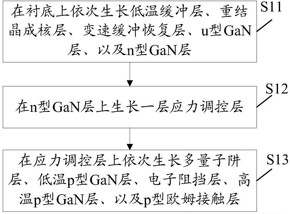
[0031] An embodiment of the present invention provides a method for preparing GaN-based light-emitting diode epitaxial wafers, which is suitable for preparing GaN-based light-emitting diode epitaxial wafers that emit blue-green light. See figure 1 , the method includes:

[0032] Step S11 , growing a low temperature buffer layer, a recrystallization nucleation layer, a variable speed buffer recovery layer, a u-type GaN layer, and an n-type GaN layer sequentially on the substrate.

[0033] In this embodiment, a sapphire substrate is used.

[0034] Step S12, growing a stress control layer on the n-type GaN layer.

[0035] Specifically, the stress regulating layer is a multi-period structure, and each period of growing the multi-period structure includes:

[0036] growing a stress-regulating InGaN sublayer at a first growth temperature;

[0037] After the growth of the stress-regulated InGaN sub-layer is completed, hydrogen gas is introduced into the reaction chamber at a secon...

Embodiment 2

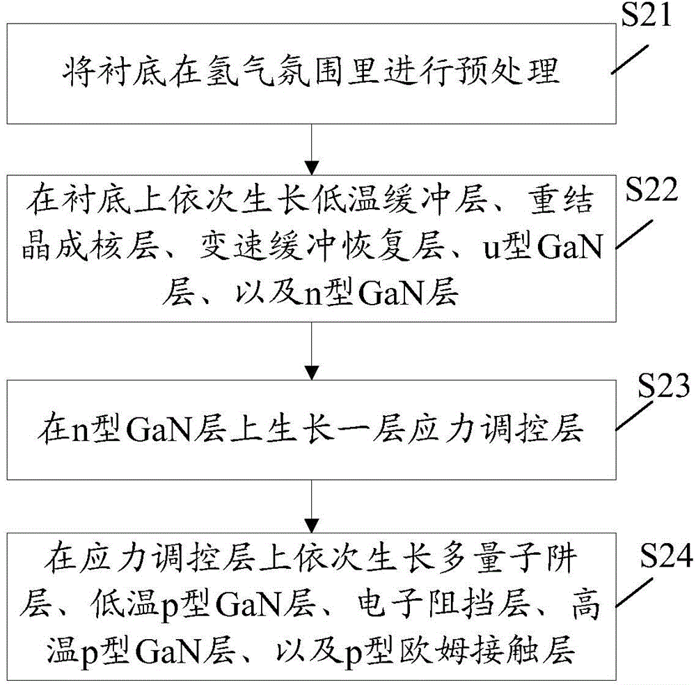
[0046] An embodiment of the present invention provides a method for preparing GaN-based light-emitting diode epitaxial wafers, which is suitable for preparing GaN-based light-emitting diode epitaxial wafers that emit blue-green light. See figure 2 , the method includes:

[0047] In step S21, the substrate is pretreated in a hydrogen atmosphere.

[0048] Specifically, the sapphire substrate is annealed in a hydrogen atmosphere for 1-10 minutes, the surface of the substrate is cleaned, and the temperature of the reaction chamber is raised to 1000-1200° C. to preheat the substrate.

[0049] Step S22 , growing a low temperature buffer layer, a recrystallization nucleation layer, a variable speed buffer recovery layer, a u-type GaN layer, and an n-type GaN layer on the substrate in sequence.

[0050] In this embodiment, a sapphire substrate is used.

[0051] Step S23 , growing a stress regulation layer on the n-type GaN layer.

[0052] Specifically, the stress regulating layer ...

Embodiment 3

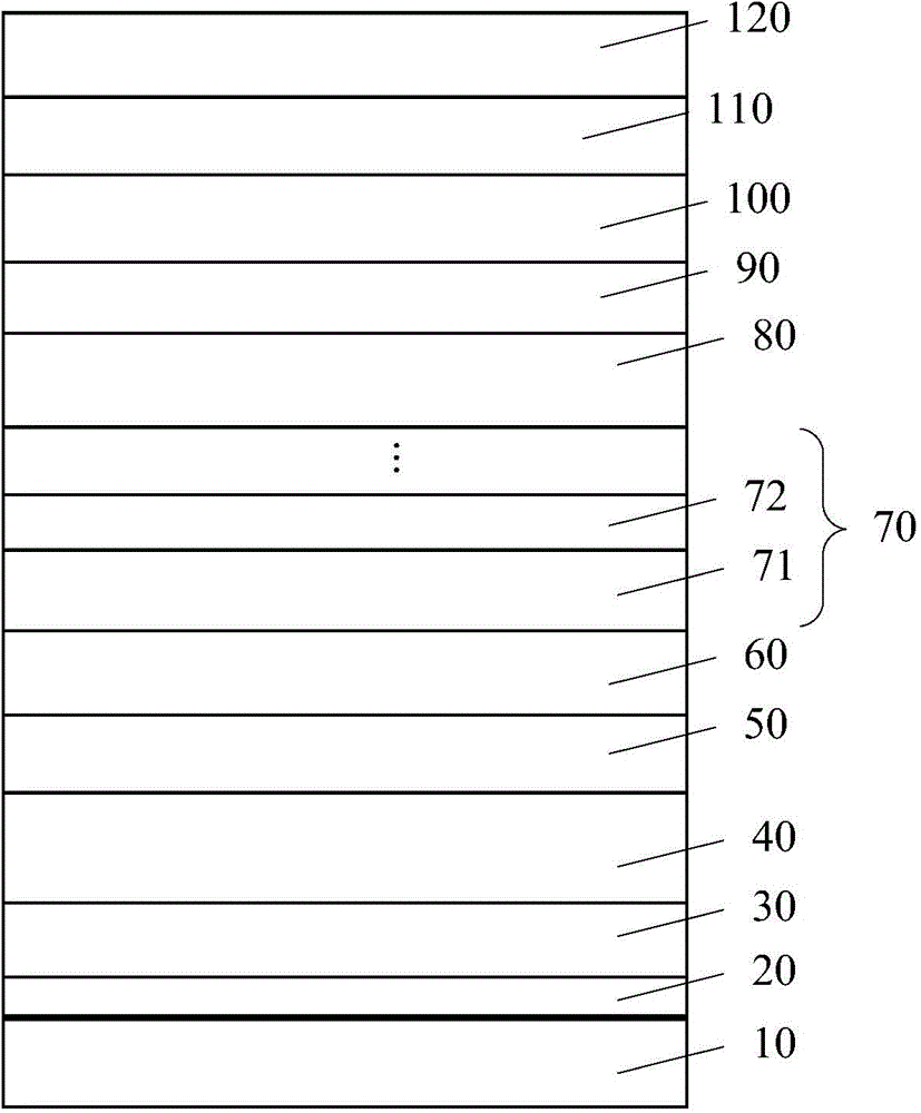
[0086] An embodiment of the present invention provides a GaN-based light-emitting diode epitaxial wafer, which can be prepared by the method described in Embodiment 1 or Embodiment 2, see image 3 , the epitaxial wafer includes: a substrate 10 and a low-temperature buffer layer 20 sequentially covered on the substrate 10, a recrystallization nucleation layer 30, a variable speed buffer recovery layer 40, a u-type GaN layer 50, an n-type GaN layer 60, a multi-quantum Well layer 80 , low temperature p-type GaN layer 90 , electron blocking layer 100 , high temperature p-type GaN layer 110 , and p-type ohmic contact layer 120 .

[0087] The epitaxial wafer also includes: a stress regulation layer 70 disposed between the n-type GaN layer 60 and the multi-quantum well layer 80, the stress regulation layer 70 is a multi-period structure, and each period of the multi-period structure includes: The stress-regulating InGaN sublayer 71 grown at the growth temperature and subjected to etc...


PUM


Abstract

The invention discloses a GaN-based light-emitting diode epitaxial wafer production method and a produced epitaxial wafer, and belongs to the field of semiconductor light-emitting diodes. The method includes growing a buffer layer, an n-type GaN layer, a stress regulation layer, a multiple quantum well layer, a p-type GaN layer and a p-type ohmic contact layer on a substrate sequentially. The stress regulation layer is of a multi-period structure. A growth method of each period of the multi-period structure includes growing a stress regulation InGaN sub layer at a first growth temperature, supplying hydrogen into a reaction chamber at a second growth temperature after the stress regulation InGaN sub layer finishes growing, and etching the surface of the stress regulation InGaN sub layer, wherein the second growth temperature is different from the first growth temperature. The GaN-based light-emitting diode epitaxial wafer production method and the produced epitaxial wafer have the advantages that through treatment of the stress regulation InGaN sub layer, a smooth contact surface is formed between the stress regulation InGaN sub layer and a stress regulation GaN sub layer, and accordingly, continuous extension of defects is prevented.

Description

technical field [0001] The invention relates to the field of semiconductor light-emitting diodes, in particular to a method for preparing GaN-based light-emitting diode epitaxial wafers and the prepared epitaxial wafers. Background technique [0002] Semiconductor light-emitting diodes (Light-Emitting Diodes, referred to as "LEDs") have attracted much attention due to their excellent characteristics, such as energy saving, environmental protection, high reliability, and long service life. In recent years, with the widespread application of LEDs, it is becoming more and more important to increase the luminous efficiency of LEDs. [0003] The structure of a conventional GaN-based LED epitaxial wafer includes: a substrate and an epitaxial layer composed of a buffer layer, an N-type gallium nitride layer, a multi-quantum well layer, and a P-type gallium nitride layer. [0004] In the process of realizing the present invention, the inventor finds that there are at least the foll...

Claims


Application Information

Patent Timeline
Patent Type & Authority Applications(China)
IPC IPC(8): H01L33/20H01L33/32H01L33/00
CPCH01L33/0066H01L33/0075H01L33/12H01L33/32
Inventor 王群郭炳磊葛永晖董彬忠李鹏王江波
Owner HC SEMITEK SUZHOU
Why Eureka
Try Eureka