Charge pump circuit suitable for low voltage operation

A charge pump and circuit technology, applied in the direction of conversion equipment without intermediate conversion to AC, can solve the problems of shortening the effective opening time of M0, occupying charge transfer time, and complex circuit implementation, so as to avoid parasitic bipolar transistor effect and reduce The effect of reverse current and layout area reduction

Active Publication Date: 2015-07-29
GIANTEC SEMICON LTD
View PDF2 Cites 3 Cited by
  • Summary
  • Abstract
  • Description
  • Claims
  • Application Information

AI Technical Summary

Problems solved by technology

The timing of the four-phase clock needs to be carefully adjusted, and it is sensitive to deviations in process and voltage. The circuit implementation is relatively complicated, and the clock overlap area for charging Cb will occupy the overall charge transfer time, making the effective turn-on time of M0 shorten

Method used


Image

  • Charge pump circuit suitable for low voltage operation
  • Charge pump circuit suitable for low voltage operation
  • Charge pump circuit suitable for low voltage operation

Examples


Embodiment Construction

[0037] In order to make the technical means, features and effects realized by the present invention easy to understand, further description will be given below in conjunction with the drawings. These descriptions and illustrations of embodiments should not be construed as limitations of the present invention. Obvious changes to the characteristics of the examples of the present invention and the extension of its application principles will also fall within the protection scope of the present invention.

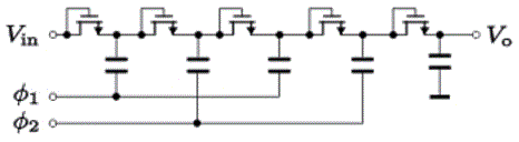
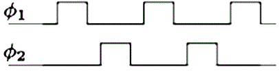
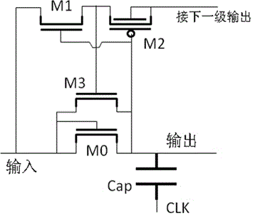
[0038] A charge pump circuit provided by the present invention improves the Dickson charge pump circuit, which can provide the required operating voltage for non-volatile memory integrated circuits, such as being used in EEPROM or flash memory chips, to generate programming and High voltage required for erasing and writing. Each charge pump circuit includes several charge pump subunits cascaded.

[0039] Such as Figure 6 Shown is the charge pump subunit of any stage provid...


PUM


Abstract

The invention relates to a charge pump circuit, wherein each level charge pump subunit is provided with four NMOS (N-channel metal oxide semiconductor) transistors and a pair of phase complementary two-phase clock signals. The charge pump circuit suitable for low voltage operation is characterized in that a drain electrode of the first transistor is connected to the input end of the level of charge pump subunit, and a source electrode is connected to the output end of level of charge pump subunit; a drain electrode of the second transistor is connected to the input end of the level of charge pump subunit; a drain electrode and a grid electrode of the third transistor are connected to the source electrode of the second transistor; a source electrode of the third transistor is connected with the grid electrode of the first transistor; a drain electrode and a grid electrode of the fourth transistor are connected to the grid electrode of the first transistor; the source electrode of the fourth transistor is connected to the input end of the level of charge pump subunit; the first-phase clock signal is connected to the output end of the level of charge pump subunit through a first capacitor and is connected to a second source electrode of the second transistor through a third capacitor; the second-phase clock signal is connected to the grid electrode of the first transistor through a second capacitor. The charge pump circuit suitable for low voltage operation can improve the voltage of the grid electrodes of NMOS transistor switches and reduce the side effect of the substrate bias effect.

Description

technical field [0001] The invention relates to a semiconductor integrated circuit, in particular to a charge pump circuit used in an EEPROM or a flash memory chip for generating high voltage. Background technique [0002] With the rise of handheld devices and the Internet of Things, the demand for integrated circuit miniaturization and energy-saving design is becoming more and more urgent, which puts forward requirements for the design of low power supply voltage of semiconductor integrated circuits. Because EEPROM and flash memory devices have the characteristics of flexible data rewriting, stored data content will not be lost after power failure, and can be kept for a long time, they are more and more widely used in the system. [0003] In CMOS EEPROM or flash memory devices, whether based on floating gate technology or charge trap technology, a high voltage generation circuit is usually required to provide the high voltage required for programming and erasing operations....

Claims


Application Information

Patent Timeline
Patent Type & Authority Applications(China)
IPC IPC(8): H02M3/07
Inventor 袁庆鹏
Owner GIANTEC SEMICON LTD
Why Eureka
Try Eureka