Simple Charge Pump Circuit for Low Voltage Operation

A charge pump and low-voltage technology, which is applied in the field of semiconductor integrated circuits, can solve the problems of complicated circuit implementation, shortened effective opening time of M0, occupied charge transfer time, etc., and achieves reduced layout area, simplified circuit and layout structure, and reduced reverse current Effect

Active Publication Date: 2017-07-11
GIANTEC SEMICON LTD
View PDF3 Cites 0 Cited by
  • Summary
  • Abstract
  • Description
  • Claims
  • Application Information

AI Technical Summary

Problems solved by technology

The timing of the four-phase clock needs to be carefully adjusted, and it is sensitive to deviations in process and voltage. The circuit implementation is relatively complicated, and the clock overlap area for charging the capacitor Cb will occupy the overall charge transfer time, so that M0 can be effectively turned on. shortened time

Method used


Image

  • Simple Charge Pump Circuit for Low Voltage Operation
  • Simple Charge Pump Circuit for Low Voltage Operation
  • Simple Charge Pump Circuit for Low Voltage Operation

Examples


Embodiment Construction

[0027] For the technical means that the present invention realizes, feature and effect are easy to understand, combine below Figure 6 and Figure 7 for further clarification. These descriptions and illustrations of embodiments should not be construed as limitations of the present invention. Obvious changes to the characteristics of the examples of the present invention and the extension of its application principles will also fall within the protection scope of the present invention.

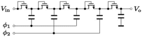
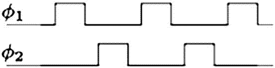
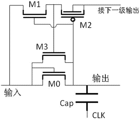
[0028] A simple charge pump circuit provided by the present invention is an improvement to the Dickson charge pump circuit, which can provide the required operating voltage for non-volatile memory integrated circuits, such as being used in EEPROM or flash memory chips, to generate by low voltage operation High voltage required for programming and erasing.

[0029] The simple charge pump circuit suitable for low-voltage operation provided by the present invention includes several charge pump ...


PUM


Abstract

The invention relates to a simple charge pump circuit suitable for low voltage operation. The simple charge pump circuit comprises a plurality of cascaded charge pump subunits; each level of charge pump subunit is provided with three NMOS (N-channel metal oxide semiconductor) transistors and a pair of two-phase clock signals. Each level of charge pump subunit comprises a first NMOS transistor, a second NMOS transistor, a third NMOS transistor, a first-phase clock signal and a second-phase clock signal, wherein the first NMOS transistor serves as a transmission switch, the drain electrode of the first NMOS transistor is connected with the input end of the level of charge pump subunit, and the source electrode of the first NMOS transistor is connected with the output end of the level of charge pump subunit; the drain electrode and the grid electrode of the NMOS transistor are connected with each other and are connected to the output end of the level of charge pump subunit, and the source electrode is connected with the grid electrode of the first NMOS transistor; the drain electrode and the grid electrode of the third NMOS transistor are connected with each other and are connected to the grid electrode of the first NMOS transistor, and the source electrode is connected with the input end of the level of charge pump subunit; the first-phase clock signal is connected with the output end of the level of charge pump subunit through a first capacitor, and the second-phase clock signal is connected with the grid electrode of the first NMOS transistor through a second capacitor. The simple charge pump circuit suitable for low voltage operation improves the voltage of the grid electrodes of the NMOS transistors serving as the transmission switches with a simple structure, reduces the side effect of the substrate bias effect and simplifies the circuit board diagram design.

Description

technical field [0001] The invention relates to a semiconductor integrated circuit, in particular to a charge pump circuit for generating high voltage in an EEPROM (Electrically Erasable Programmable Read-Only Memory, Electrically Erasable Programmable Read-Only Memory) or a flash memory chip. Background technique [0002] With the rise of handheld devices and the Internet of Things, the demand for integrated circuit miniaturization and energy-saving design is becoming more and more urgent, which puts forward requirements for the design of low power supply voltage of semiconductor integrated circuits. Because EEPROM and flash memory devices have the characteristics of flexible data rewriting, stored data content will not be lost after power failure, and can be kept for a long time, they are more and more widely used in the system. [0003] In CMOS EEPROM or flash memory devices, whether based on floating gate technology or charge trap technology, a high voltage generation ci...

Claims


Application Information

Patent Timeline
Patent Type & Authority Patents(China)
IPC IPC(8): H02M3/07
CPCH02M3/07
Inventor 袁庆鹏
Owner GIANTEC SEMICON LTD
Why Eureka
Try Eureka