EEPROM memory device and preparation method thereof
A storage device and control gate technology, which is applied in semiconductor/solid-state device manufacturing, electric solid-state devices, semiconductor devices, etc., can solve the problems of device size increase, process complexity, device damage, etc., and achieve device size reduction and increase process window , Increase the effect of process margin
- Summary
- Abstract
- Description
- Claims
- Application Information
AI Technical Summary
Problems solved by technology
Method used
Image

Examples
preparation example Construction
[0051] The present invention provides a kind of preparation method of EEPROM device in order to solve the problem existing in the prior art, comprising:
[0052] providing a semiconductor substrate, on which a gate of a high-voltage transistor and a floating gate of a storage device are formed;
[0053] depositing a gate dielectric layer on the gate of the high voltage transistor and the floating gate;
[0054] depositing a control gate material layer on the gate dielectric layer;
[0055] Etching the control gate material layer and the gate dielectric layer to form a control gate above the floating gate, and at the same time forming a gate formed by the control gate material layer on the sidewall of the gate of the high voltage transistor. first spacer;
[0056] A second spacer is formed on the first spacer of the gate of the high voltage transistor and on the sidewall of the control gate.
Embodiment 1
[0058] Attached below Figure 2a-2d The embodiments of the present invention will be further described.
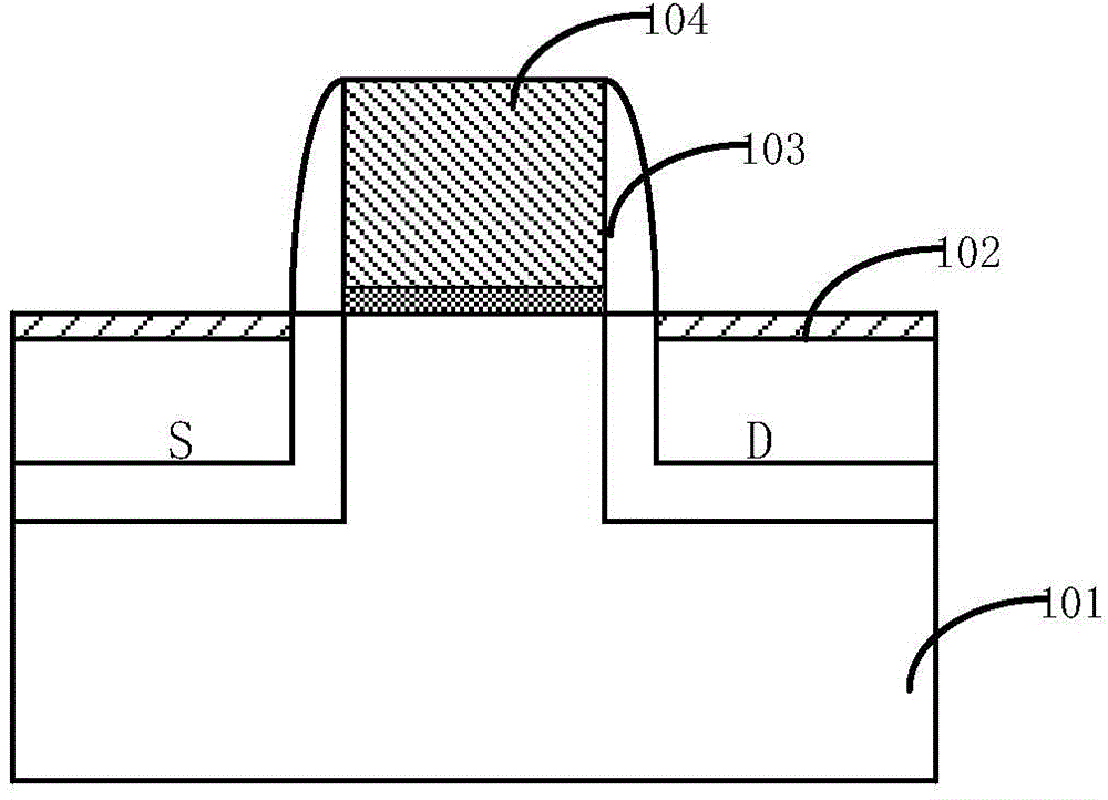
[0059] First, step 201 is performed to provide a semiconductor substrate 201, on which a gate 204 of a high-voltage transistor formed of a layer of semiconductor material and a floating gate 203 of a control gate are formed, and the gate 204 of the high-voltage transistor A gate dielectric layer 205 and a control gate material layer 206 are also formed on the floating gate 203 .
[0060] Specifically, as Figure 2a As shown, a semiconductor substrate 201 is provided, and the semiconductor substrate 201 may be at least one of the materials mentioned below: silicon, silicon-on-insulator (SOI), silicon-on-insulator (SSOI), germanium-on-insulator Silicon-on-insulator (S-SiGeOI), silicon-germanium-on-insulator (SiGeOI), and germanium-on-insulator (GeOI).
[0061] In addition, other devices may be formed on the semiconductor substrate 201 , for example, an isolation structure...
Embodiment 2
[0080] Combine below Figures 3a-3i A preferred embodiment of the present invention will be further described.
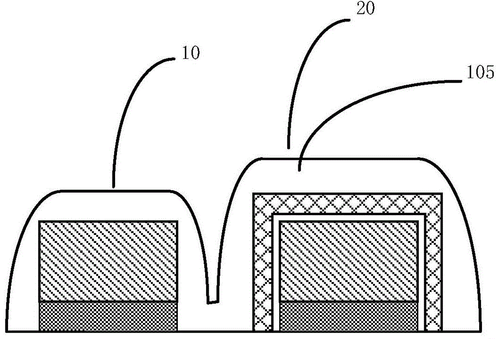
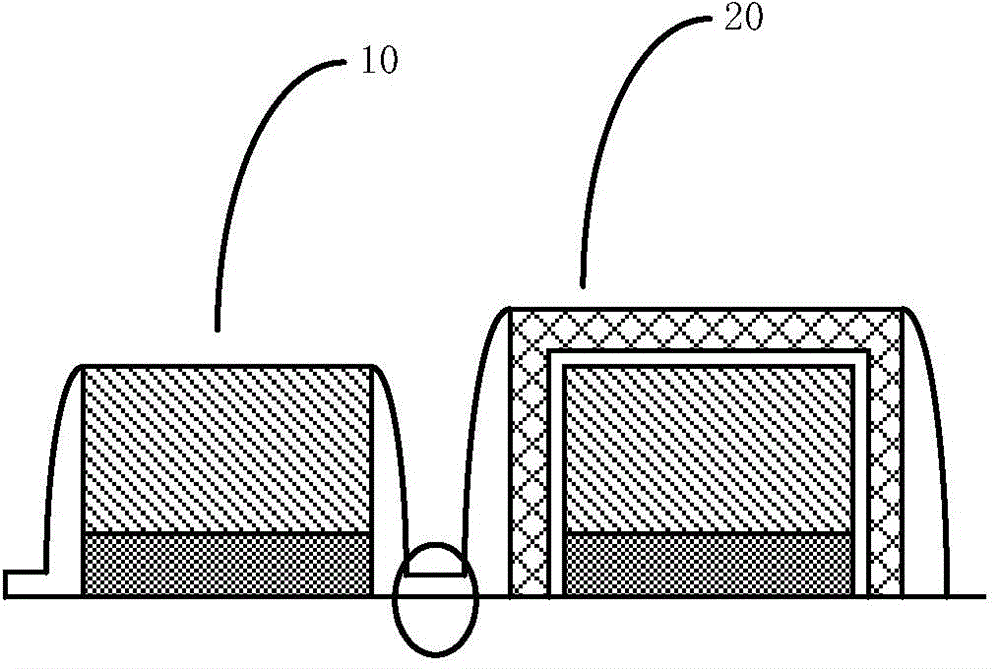
[0081] It should be noted that, in the EEPROM device, a typical split-gate structure EEPROM includes a control gate, a floating gate on the control gate, and a gate of a discrete high-voltage transistor. But when Figures 3a-3i Only the gate of the high-voltage transistor is shown in the figure, and the control gate is not drawn, but it should be noted that during the device preparation process, on the same wafer, there are many processes in the preparation process of the control gate and the gate of the high-voltage transistor. The process steps are completed together, such as the source and drain implantation and the etching of the spacer. In the absence of special instructions, although the preparation process of the control gate will not be involved in the following description, the actual process will be in the same step. Complete some structures in, as shown...
PUM
 Abstract
Description
Claims
Application Information
 - R&D
- Intellectual Property
- Life Sciences
- Materials
- Tech Scout
- Unparalleled Data Quality
- Higher Quality Content
- 60% Fewer Hallucinations
Browse by: Latest US Patents, China's latest patents, Technical Efficacy Thesaurus, Application Domain, Technology Topic, Popular Technical Reports.
© 2025 PatSnap. All rights reserved.Legal|Privacy policy|Modern Slavery Act Transparency Statement|Sitemap|About US| Contact US: help@patsnap.com