Thin-film transistor and manufacturing method thereof, array substrate and display device
What is Al technical title?
Al technical title is built by PatSnap Al team. It summarizes the technical point description of the patent document.
A technology of thin film transistors and manufacturing methods, applied in the direction of transistors, semiconductor/solid-state device manufacturing, electric solid-state devices, etc., can solve the problems of display aperture ratio decrease, off-state current difficult to maintain, TFT area increase, etc., to reduce photoleakage current, increase the band gap, and reduce the effect of leakage current
Inactive Publication Date: 2015-08-26
TRULY HUIZHOU SMART DISPLAY
View PDF4 Cites 3 Cited by
Summary
Abstract
Description
Claims
Application Information
AI Technical Summary
This helps you quickly interpret patents by identifying the three key elements:
Problems solved by technology
Method used
Benefits of technology
Problems solved by technology
However, the negative impact of these methods is that the TFT area increases significantly and the aperture ratio of the display decreases
In high-resolution displays, as the resolution increases, the area of each pixel becomes smaller and smaller. In a limited pixel area, the off-state current of the polysilicon thin film transistor is reduced by increasing the channel length of the TFT. The disadvantages are also becoming more and more obvious and difficult to maintain
Method used
Image
Click on the blue label to locate the original text in one second.
Reading with bidirectional positioning of images and text.
Examples
Embodiment Construction
[0046] In order to further understand the features, technical means and specific objectives and functions achieved by the present invention, the present invention will be further described in detail below in conjunction with specific embodiments.
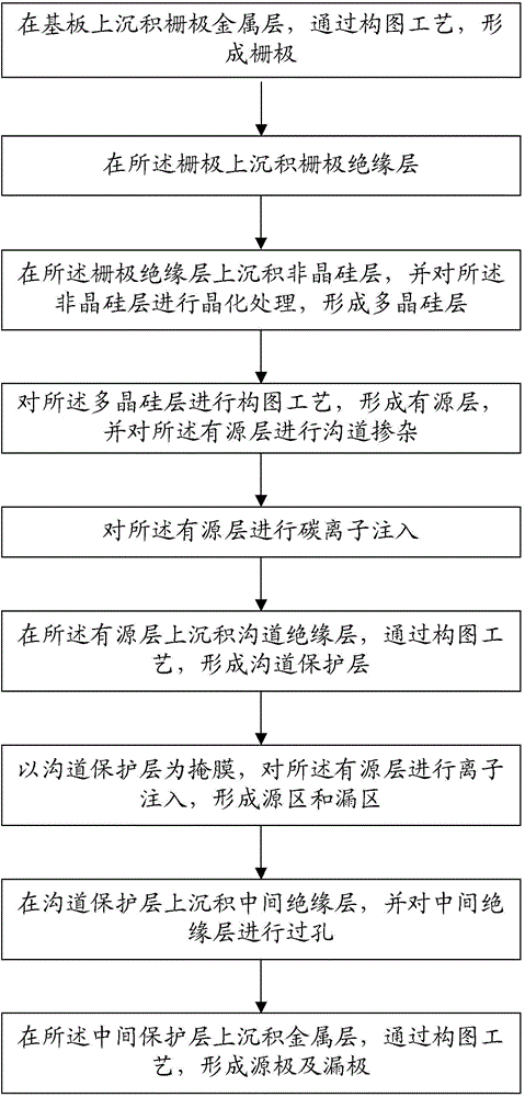
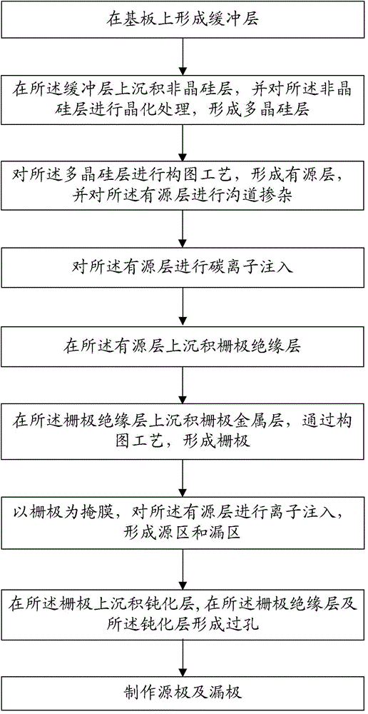
[0047] For example, a method for manufacturing a thin film transistor includes: a step of depositing an amorphous silicon layer; a step of crystallizing the amorphous silicon layer to form a polysilicon layer; a step of forming an active layer; forming a channel doped the step of carbon ion implantation; the step of forming gate insulating layer and gate; the step of forming via hole; the step of forming source electrode and drain electrode. As another example, the step of forming the polysilicon layer is followed by the step of implanting carbon ions. That is, carbon ion implantation is performed on the polysilicon layer. In another example, after forming the active layer, the step of carbon ion implantation is performed, and then...
PUM
Abstract
The invention provides a manufacturing method of a thin-film transistor. The method comprises a step of deposition of an amorphous silicon layer; a step of formation of a polycrystalline silicon layer through crystallizing treatment; a step of formation of an active layer; a step of formation of channel doping; a step of carbon ion injection; a step of formation of via holes; a step of formation of a gate electrode insulating layer and a gate electrode; and a step of formation of a source electrode and a drain electrode. According to the manufacturing method of the thin-film transistor, forbidden bandwidth of the active layer can be enhanced and thus leakage current of a low-temperature polycrystalline silicon thin-film transistor can be reduced. Besides, visible light absorption coefficient of low-temperature polycrystalline silicon can also be reduced, and light-induced leakage current generated by a backlight source can be reduced. Furthermore, the manufacturing method of the thin-film transistor is suitable for existing polycrystalline silicon thin-film transistor production lines without additional number of times of photo-masking or modification of production equipment, and thus the operation method is easy and convenient. The invention also provides the thin-film transistor, an array substrate and a display device.
Description
technical field [0001] The invention relates to the field of semiconductor devices, in particular to a thin film transistor and a manufacturing method thereof, an array substrate and a display device. Background technique [0002] Thin film transistor liquid crystal display (TFT-LCD) is the most important type in the field of flat panel display, because it has many advantages, such as thin size, light weight, excellent picture quality, low power consumption, long life, digital, etc., and it is also the only Display technology that spans all sizes, and its application fields are very wide, covering almost the main electronic products in today's information society, such as TV, monitor, portable computer, mobile phone, PDA, GPS, vehicle display, instrumentation, public display and medical display etc. [0003] In liquid crystal displays, thin film transistors are generally used as switching elements to control pixels, or as driving elements to drive pixels. Thin film transis...
Claims
Application Information
Patent Timeline
Application Date:The date an application was filed.
Publication Date:The date a patent or application was officially published.
First Publication Date:The earliest publication date of a patent with the same application number.
Issue Date:Publication date of the patent grant document.
PCT Entry Date:The Entry date of PCT National Phase.
Estimated Expiry Date:The statutory expiry date of a patent right according to the Patent Law, and it is the longest term of protection that the patent right can achieve without the termination of the patent right due to other reasons(Term extension factor has been taken into account ).
Invalid Date:Actual expiry date is based on effective date or publication date of legal transaction data of invalid patent.