Adjustable vertical magneto-resistor element
A magneto-resistance and element technology, applied in the field of vertical magneto-resistance elements, can solve problems such as inability to obtain thermal stability of demagnetization effect
- Summary
- Abstract
- Description
- Claims
- Application Information
AI Technical Summary
Problems solved by technology
Method used
Image
Examples
Embodiment 1
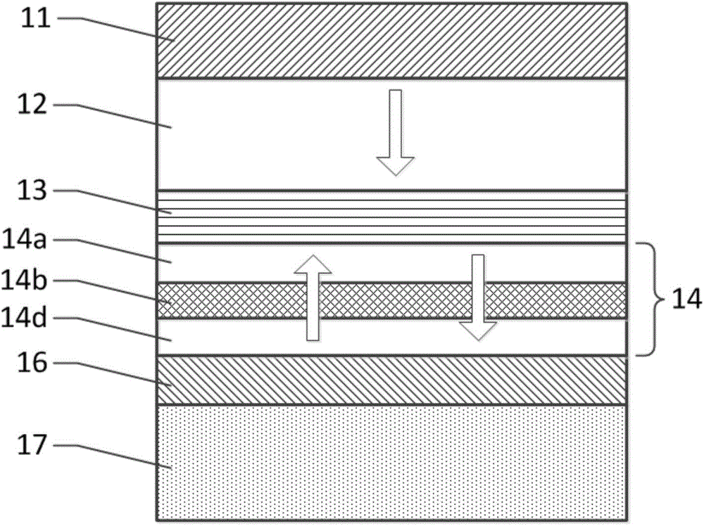
[0035] figure 1 It is a structural diagram of an MTJ element based on the present invention, which includes a top electrode 11, a reference layer 12, a barrier layer 13, a memory layer 14, a functional layer 16 and a bottom electrode 17 arranged adjacently from top to bottom, wherein the memory Layer 14 is composed of sequentially adjacent first memory sublayer 14a, intermediate memory layer 14b and second memory sublayer 14d.
[0036] The reference layer 12 and the memory layer 14 are ferromagnetic materials, the magnetization direction of the reference layer 12 is constant and the magnetic anisotropy is perpendicular to the layer surface, and the magnetization direction of the memory layer 14 is variable and the magnetic anisotropy is perpendicular to the layer surface. The magnetic perpendicular anisotropy energy of the reference layer 12 is sufficiently greater than the magnetic perpendicular anisotropy energy of the memory layer 14, which can be realized by adjusting the ...
Embodiment 2
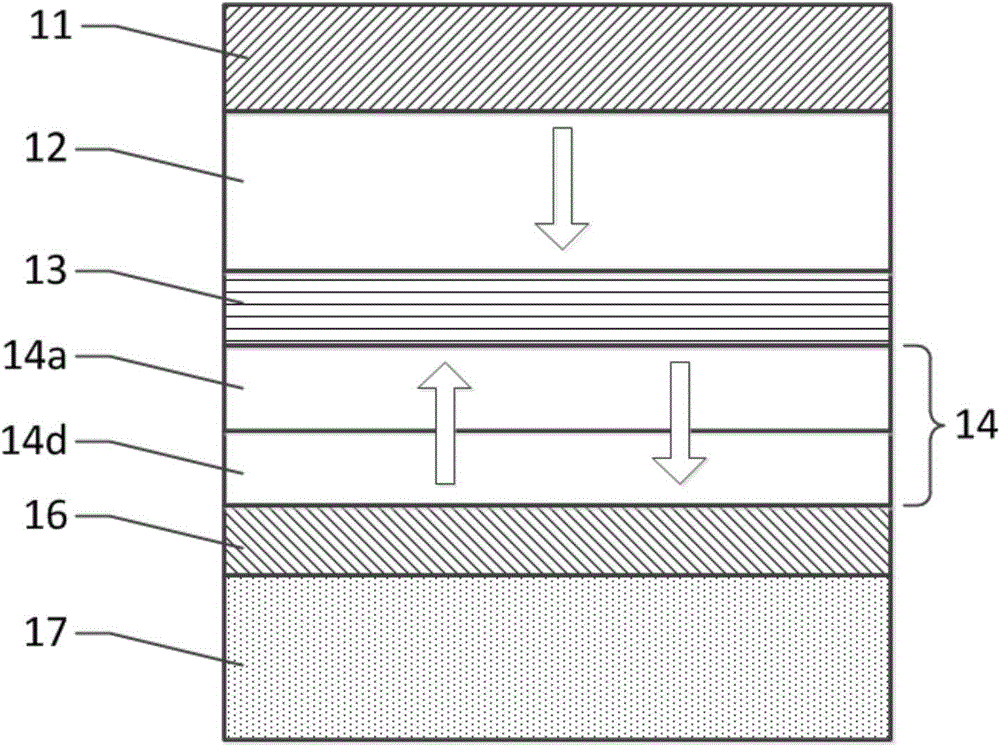
[0044] figure 2 It is a structural schematic diagram of another MTJ element based on the present invention, which includes a top electrode 11, a reference layer 12, a barrier layer 13, a memory layer 14, a functional layer 16 and a bottom electrode 17 arranged adjacently in order from top to bottom, wherein The memory layer 14 is composed of a first memory sublayer 14a and a second memory sublayer 14d which are sequentially adjacent.
[0045] Compared with Embodiment 1, the difference of this embodiment lies only in the setting of the memory layer 14 . Wherein, the memory layer 14 has a double-layer structure, and the first memory sub-layer 14a is made of semi-metallic Heusler alloy, preferably Co2MnSi, Co2FeAl, Co2FeSi or Co2MnAl. In this embodiment, the material of the first memory sublayer 14a is a semimetal Heusler alloy Co2FeAl (thickness is about 2.5nm); the material of the second memory sublayer 14d is CoFeB (thickness is about 1.2nm), wherein the B content is 20%.
Embodiment 3
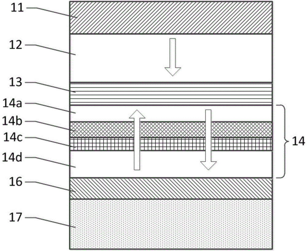
[0047] image 3 is in figure 1 A schematic diagram of the structure of an MTJ element further improved on the basis of the device structure in the middle, including a top electrode 11, a reference layer 12, a barrier layer 13, a memory layer 14, a functional layer 16 and a bottom electrode 17 arranged adjacently in sequence from top to bottom , wherein the memory layer 14 is composed of sequentially adjacent first memory sublayer 14a, middle memory layer 14b, insertion layer 14c and second memory sublayer 14d. and figure 1 The difference in device structure is that an insertion layer 14c is added between the middle memory layer 14b and the second memory sublayer 14d.
[0048] The material of the insertion layer 14c is preferably Ta, W, Ti, Cr, Zr, Nb, Hf, V, Mo, Pt, Pd, Au, Ag or Al, and Ta (with a thickness of about 0.3 nm) is used in this embodiment. When heat treatment is performed on the MTJ, the B atoms in the optimization layer 14 will also diffuse into the insertion ...
PUM
 Abstract
Description
Claims
Application Information


