Heterojunction spinning field effect transistor based on 4H-SiC substrate, and manufacturing method for heterojunction spinning field effect transistor

A field-effect transistor and heterojunction technology, which is applied in the manufacture of semiconductor/solid-state devices, semiconductor devices, electrical components, etc., can solve the problem that the efficiency of spin injection is only a few percent, and achieve the optimization of spin polarizability Effect

Active Publication Date: 2017-11-21
XIDIAN UNIV
View PDF6 Cites 1 Cited by
  • Summary
  • Abstract
  • Description
  • Claims
  • Application Information

AI Technical Summary

Problems solved by technology

[0004] However, the general spin field effect transistor injects spin electrons into the semiconductor by ferromagnetic materials, and the efficiency of spin injection is only a few percent due to the mismatch between the energy band structures of ferromagnetic materials such as Fe and semiconductor materials such as Sm.

Method used


Image

  • Heterojunction spinning field effect transistor based on 4H-SiC substrate, and manufacturing method for heterojunction spinning field effect transistor
  • Heterojunction spinning field effect transistor based on 4H-SiC substrate, and manufacturing method for heterojunction spinning field effect transistor
  • Heterojunction spinning field effect transistor based on 4H-SiC substrate, and manufacturing method for heterojunction spinning field effect transistor

Examples


Embodiment 1

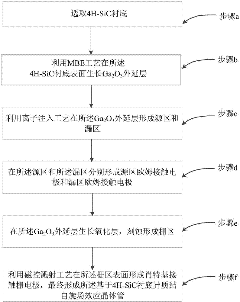
[0047] See figure 1 , figure 1A schematic diagram of a heterojunction spin field effect transistor based on a 4H-SiC substrate and a manufacturing method thereof provided by an embodiment of the present invention. The method comprises the steps of:

[0048] Step a, select 4H-SiC substrate;

[0049] Step b, using the MBE process to grow Ga on the surface of the 4H-SiC substrate 2 o 3 epitaxial layer;

[0050] Step c, using an ion implantation process on the Ga 2 o 3 The epitaxial layer forms source and drain regions;

[0051] Step d, forming a source region ohmic contact electrode and a drain region ohmic contact electrode in the source region and the drain region respectively;

[0052] Step e, in the Ga 2 o 3 The oxide layer is grown on the epitaxial layer, and the gate area is formed by etching;

[0053] Step f, using a magnetron sputtering process to form a Schottky contact gate electrode on the surface of the gate region, and finally forming the heterojunction sp...

Embodiment 2

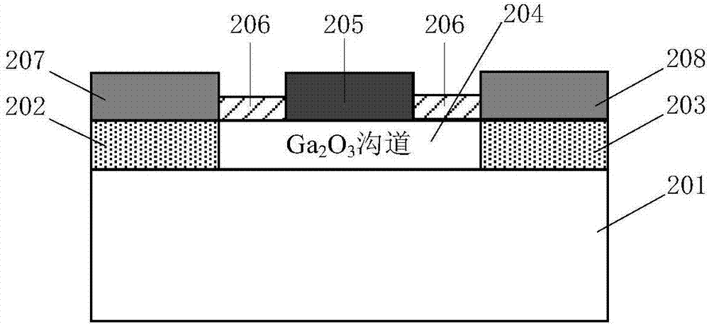
[0076] See figure 2 , figure 2 A device schematic diagram of a heterojunction spin field effect transistor based on a 4H-SiC substrate provided by an embodiment of the present invention. The heterojunction spin field effect transistor based on 4H-SiC substrate includes: 4H-SiC substrate 201, Fe-doped Ga 2 o 3 Source region 202, Fe-doped Ga 2 o 3 Drain region 203, Ga 2 o 3 Channel region 204, Schottky contact gate electrode 205, SiO 2 The isolation layer 206, the ohmic contact source 207, and the ohmic contact drain 208, the heterojunction spin field effect transistor based on the 4H-SiC substrate is prepared and formed by the method described in the above-mentioned embodiments.

[0077] The machine manufacturing method of the heterojunction high electron mobility spin field effect transistor of the present invention, because the same material is used for the channel and the source and drain regions, epitaxial growth can be directly performed on the substrate, and at t...

Embodiment 3

[0079] See Figure 3a-Figure 3g A process schematic diagram of a heterojunction spin field effect transistor based on a 4H-SiC substrate provided by an embodiment of the present invention. On the basis of the above embodiments, this embodiment will introduce the process flow of the present invention in more detail. The method includes:

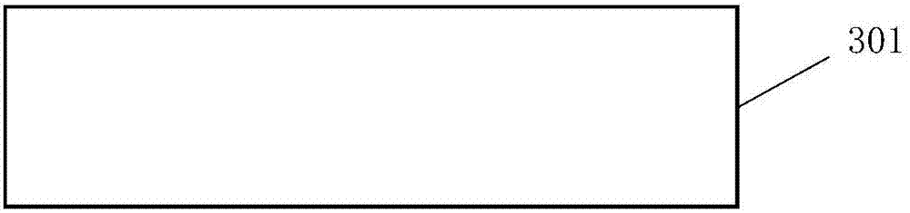
[0080] Step 301, select the 4H-SiC substrate 301, and use acetone, absolute ethanol and deionized water to perform ultrasonic cleaning on the 4H-SiC substrate, such as Figure 3a shown;

[0081] Step 302, at a temperature of 940°C, the power of the radio frequency source is 300W, and the pressure is 1.5×10 -5 Torr, the evaporation source materials Ga and Sn, the mass fractions are 99.99999% and 99.999% respectively, and the thickness is 0.4-0.6 μm grown on the surface of 4H-SiC substrate 301 by MBE process, and the doping concentration is 1×10 14 -1×10 16 cm -3 Ga 2 o 3 Epitaxial layer 302, such as Figure 3b shown;

[0082] Preferab...


PUM


Abstract

The invention relates to a heterojunction spinning field effect transistor based on a 4H-SiC substrate, and a manufacturing method for the heterojunction spinning field effect transistor. The method comprises the following steps: selecting the 4H-SiC substrate; growing a Ga2O3 epitaxial layer on the surface of the 4H-SiC substrate through employing the MBE technology; forming a source region and a drain region on the Ga2O3 epitaxial layer through the ion implantation technology; respectively forming a source region ohmic contact electrode and a drain region ohmic contact electrode in the resource region and the drain region; growing an oxidation layer on the Ga2O3 epitaxial layer, and carrying out the etching to form a grid region; forming a Schottky contact grid electrode on the surface of the grid region through the technology of magnetron sputtering, and finally forming the heterojunction spinning field effect transistor based on the4H-SiC substrate. According to the invention, the source and drain regions are formed in a mode of selecting regions and carrying out the implantation of Fe ions. The method is compatible with the conventional technology, is simple in manufacturing, is small in surface effect, and can improve the spinning injection and receiving efficiency.

Description

technical field [0001] The invention relates to the technical field of integrated circuits, in particular to a heterojunction spin field effect transistor based on a 4H-SiC substrate and a manufacturing method thereof. Background technique [0002] In today's information society, integrated circuits have become the basis for informationization and intelligence in all walks of life. Integrated circuits play an irreplaceable role in civilian fields such as computers, televisions, and mobile phones, and in military fields such as aerospace, interstellar flight, and weaponry. With the rapid update of modern electronic technology, the development of traditional electronic devices has severely restricted the development of microelectronics science in terms of scale integration and computing speed. The emerging spintronics aims to conveniently regulate the spin of electrons, opening up a new field of information storage and transmission by using spin of electrons, which has caused...

Claims


Application Information

Patent Timeline
Patent Type & Authority Applications(China)
IPC IPC(8): H01L29/66H01L29/812H01L21/34
CPCH01L29/66969H01L29/66984H01L29/812
Inventor 贾仁需杨宇元磊张玉明彭博
Owner XIDIAN UNIV
Why Eureka
Try Eureka