
Method of manufacturing semiconductor device

A manufacturing method and semiconductor technology, which can be applied to semiconductor lasers, light guides, structures of active regions, etc., and can solve problems such as limiting the thickness of compound semiconductor layers.

Active Publication Date: 2015-08-26
MITSUBISHI ELECTRIC CORP
View PDF6 Cites 8 Cited by
  • Summary
  • Abstract
  • Description
  • Claims
  • Application Information

AI Technical Summary

Problems solved by technology

Therefore, there is a problem that the layer thickness of the compound semiconductor layer is limited.

Method used


Image

  • Method of manufacturing semiconductor device
  • Method of manufacturing semiconductor device
  • Method of manufacturing semiconductor device

Examples


Embodiment approach 1

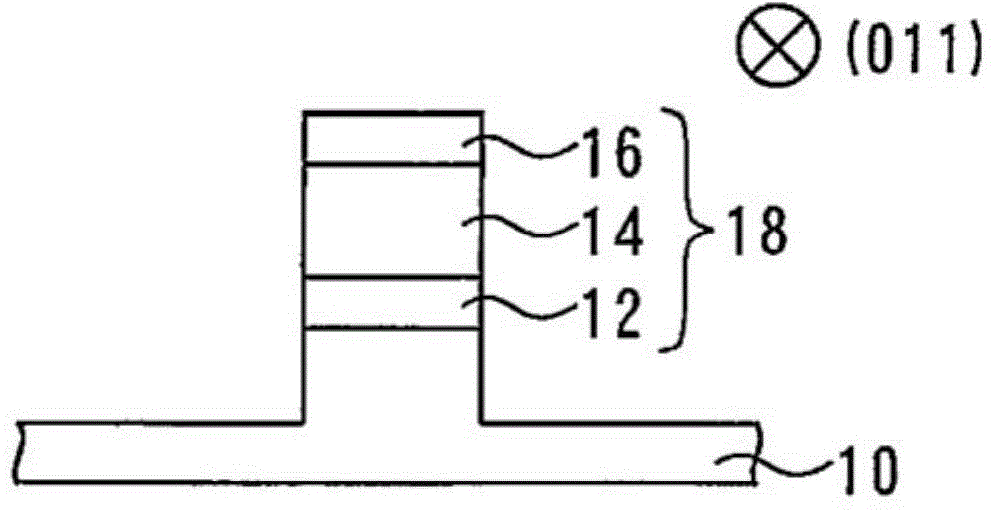
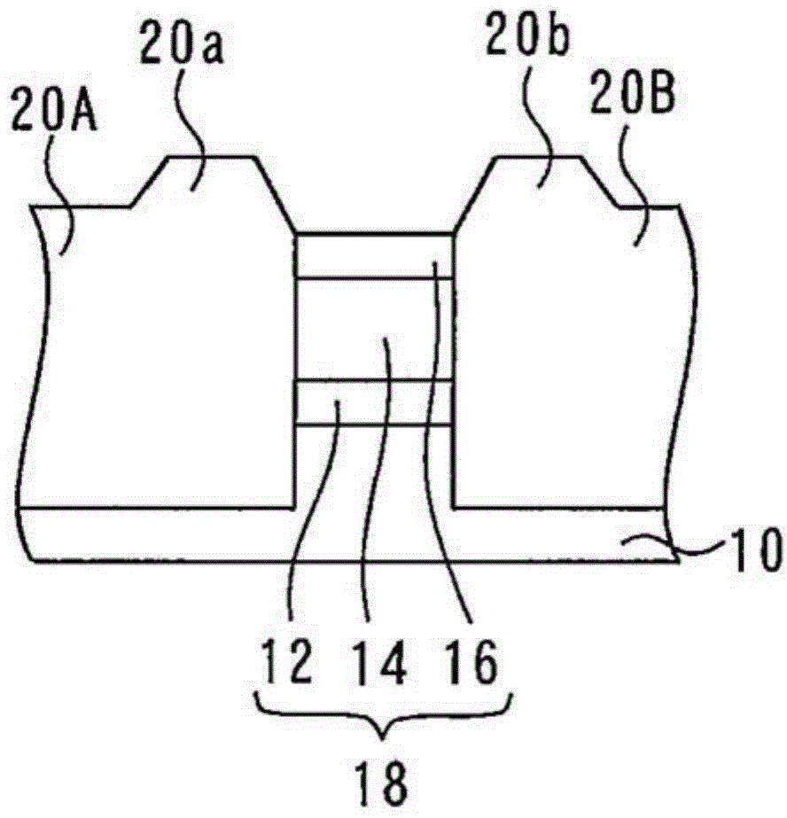
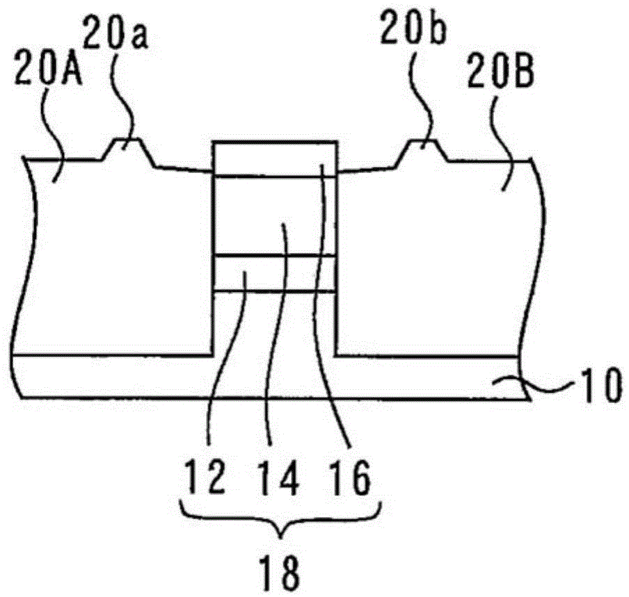
[0039] According to the method of manufacturing a semiconductor device according to Embodiment 1 of the present invention, a semiconductor device having a compound semiconductor layer functioning as a current blocking layer on the left and right of the laser portion having a raised stripe shape is formed. First, a laser portion is formed. figure 1 is a cross-sectional view showing the laser unit 18 . Substrate 10 is formed of InP. An active layer 12 is formed at a portion of the substrate 10 . The active layer 12 is formed as a multiple quantum well structure in which InGaAs quantum well layers and InGaAs barrier layers are stacked alternately and repeatedly. An upper semiconductor layer 14 made of InP is formed on the active layer 12 .

[0040] A mask 16 is formed on the upper semiconductor layer 14 . Mask 16 is formed of InGaAs. The active layer 12 , the upper semiconductor layer 14 , and the mask 16 constitute a laser section 18 . will form figure 1 The process of th...

Embodiment approach 2

[0073] In Embodiment 1, a current blocking layer is formed as a compound semiconductor layer, but in Embodiment 2, an optical modulator is formed as a compound semiconductor layer. That is, the method of manufacturing a semiconductor device according to Embodiment 2 is a method of manufacturing a laser diode with an optical modulator. First, through the laser portion forming process, a Figure 10 The laser section 18 is shown.

[0074] Then, through the semiconductor layer forming process, a Figure 11 The compound semiconductor layer 60 is shown. The compound semiconductor layer 60 constitutes an optical modulator in contact with the (011) plane or the (0-1-1) plane of the laser unit 18 . The compound semiconductor layer 60 has a cladding layer 62 formed on the substrate 10 , an active layer 64 formed on the cladding layer 62 , and a cladding layer 66 formed on the active layer 64 . These layers are formed by the MOCVD method, and therefore, convex portions 66 a are forme...

Embodiment approach 3

[0080] In the method of manufacturing a semiconductor device according to Embodiment 3, a laser diode, an optical modulator, and an optical waveguide are formed on a substrate. First, through the laser portion forming process, a Figure 14 The laser section 18 is shown. Then, the light modulator 100 is formed on the substrate 10 . The optical modulator 100 has a mask 102 formed of InGaAs on the uppermost layer.

[0081] Then, through the semiconductor layer forming process, a Figure 15 The compound semiconductor layer 104 is shown. The compound semiconductor layer 104 is in contact with the (011) plane or the (0-0-1) plane of the laser portion 18 , and is in contact with the (011) plane or the (0-0-1) plane of the optical modulator 100 . The compound semiconductor layer 104 has a cladding layer 106 made of InP, an active layer 108 made of InGaAsP / InGaAsP formed on the cladding layer 106 , and a cladding layer 110 made of InP formed on the active layer 108 . The compound ...


PUM


Abstract

A method of manufacturing a semiconductor device, includes forming a laser section on a portion of a substrate, the laser section including an active layer, an upper semiconductor layer on the active layer, and a mask on the upper semiconductor layer; forming a compound semiconductor layer of an indium-containing material in contact with a side of the laser section, the compound semiconductor layer having a projection immediately adjacent the laser section; and wet etching and removing the projection with an etchant containing hydrobromic acid and acetic acid, planarizing the compound semiconductor layer, and producing a (111)A surface in the upper semiconductor layer, under the mask.

Description

technical field [0001] The present invention relates to a method of manufacturing a semiconductor device used, for example, in optical communication or the like. Background technique [0002] Patent Document 1 discloses that when a compound semiconductor layer (InP buried layer) is epitaxially grown on the left and right sides of the raised stripes, protrusions are formed on the compound semiconductor layer. The technique disclosed in Patent Document 1 wet-etches the convex portion using an etchant composed of hydrochloric acid, acetic acid, and hydrogen peroxide. [0003] Patent Document 1: Japanese Patent Laid-Open No. 2002-246684 [0004] Since the protrusions of the compound semiconductor layer degrade the characteristics of the semiconductor device, they are preferably removed. This protrusion can be removed by wet etching. However, there is a problem that the active layer is exposed when the upper semiconductor layer which is in contact with the compound semiconduct...

Claims


Application Information

Patent Timeline
Patent Type & Authority Applications(China)
IPC IPC(8): H01S5/34
CPCH01S5/0421H01S5/026H01S5/1028H01S5/0265H01S5/34313H01S5/1007H01S5/101H01S5/1014H01S5/2201H01S5/2222H01S5/2275H01S5/3202H01S5/34306H01S5/2086G02B6/122
Inventor 津波大介河原弘幸柳乐崇
Owner MITSUBISHI ELECTRIC CORP
Learn More