Optical waveguide element and optical modulator

A technology of optical waveguide and components, applied in the field of optical modulators, can solve the problems of low light loss, difficulty in making light loss, inability to build optical communication systems, etc., and achieve the effect of low light loss

Inactive Publication Date: 2015-09-02
FUJIKURA LTD
View PDF5 Cites 23 Cited by
  • Summary
  • Abstract
  • Description
  • Claims
  • Application Information

AI Technical Summary

Problems solved by technology

As a result, if the high-order mode component is superimposed on the intensity modulation signal or the phase modulation signal, the extinction ratio of the intensity modulation or the Q value (Q-factor) of the phase modulation will decrease, and the bit error rate will increase, making it impossible to construct a good optical communication system
[0012] In the silicon Mach-Zehnder type waveguide having a PN diode disclosed in Non-Patent Document 1, it is necessary to reduce the optical loss to less than 10 dB in the wavelength region including the C-band (1530-1565 nm) and the L-band (1565-1625 nm). very difficult
Therefore, the low optical loss required for optical components for long-distance wavelength division multiplexing optical fiber communication cannot be realized

Method used


Image

  • Optical waveguide element and optical modulator
  • Optical waveguide element and optical modulator
  • Optical waveguide element and optical modulator

Examples


Embodiment

[0112] Hereinafter, the present invention will be specifically described based on examples.

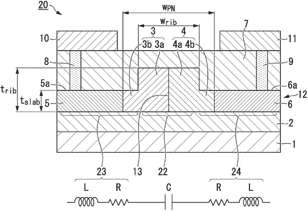
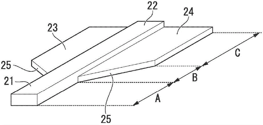
[0113] exist figure 1 In the shown structure, an SOI wafer is used as materials for the substrate 1 , the lower cover portion 2 , and the core layer 12 . The BOX layer made of silicon dioxide with a thickness of 2 μm was used as the lower cover part 2, and P-type and N-type dopants were added to the SOI layer made of silicon above it by ion implantation, thereby forming the P-type semiconductor part 3 , N-type semiconductor portion 4 , P-type conductor portion 5 , and N-type conductor portion 6 . In addition, a part of the core layer 12 was removed by etching to form the ridge portion 22 and the flat plate portions 23 and 24 . Ridge width w rib 500~600nm, ridge thickness t rib is 220nm, plate thickness t slab 95nm, the distance w between the P-type conductor part 5 and the N-type conductor part 6 PN is about 2 μm. The upper cover portion 7 made of silicon dioxide is deposited t...


PUM

PropertyMeasurementUnit
widthaaaaaaaaaa
thicknessaaaaaaaaaa
refractive indexaaaaaaaaaa

Abstract

An optical waveguide element is provided with a rib-type waveguide having a core that has a rib portion, and a pair of slab portions including a first slab portion and a second slab portion that are connected respectively to both ends of the rib portion so as to sandwich the rib portion. The rib portion has a cross-sectional dimension that allows the propagation of light of a basic mode and a high-order mode in a preset single polarization state, and has a first P-type semiconductor and a first N-type semiconductor that form a PN junction. The first slab portion has a second P-type semiconductor and a P-type conductor that are connected to each other, the second P-type semiconductor being connected to the first P-type semiconductor of the rib portion. The second slab portion has a second N-type semiconductor and an N-type conductor that are connected to each other, the second N-type semiconductor being connected to the first N-type semiconductor of the rib portion.

Description

technical field [0001] The present invention relates to a high-speed optical waveguide element with low optical loss and an optical modulator including the optical waveguide element. [0002] This application claims the priority of Japanese Patent Application No. 2012-283964 for which it applied in Japan on December 27, 2012, and uses the content here. Background technique [0003] In recent years, studies have been conducted on the use of optical integrated circuits such as substrate-type optical waveguides in devices for optical fiber communication, especially for long-distance wavelength division multiplexing optical fiber communication. [0004] Patent Document 1 discloses a single-mode silicon ridge waveguide that has a PIN junction in the lateral direction and controls the refractive index by changing the carrier density in the PIN junction. [0005] The following optical modulator is described in Patent Document 2. The optical modulator is a silicon ridge waveguide w...

Claims


Application Information

Patent Timeline
Patent Type & Authority Applications(China)
IPC IPC(8): G02F1/025G02B6/12
CPCG02F1/025G02F2001/212G02F1/2257G02F1/0152G02F1/212G02B6/1228G02B2006/12061G02B2006/12097G02B2006/12159G02F1/015
Inventor 小川宪介五井一宏日下裕幸
Owner FUJIKURA LTD
Why Eureka
Try Eureka