Preparation method and application of micro-fluidic chip based on 3D printing technique

A microfluidic chip and 3D printing technology, applied in chemical instruments and methods, laboratory containers, laboratory utensils, etc., can solve the problems of high processing technology requirements, complicated preparation process, long preparation cycle, etc., and achieve production The effect of shortening the preparation cycle, low preparation cost and low cost

Inactive Publication Date: 2015-09-09
SHANGHAI JIAO TONG UNIV
View PDF5 Cites 14 Cited by
  • Summary
  • Abstract
  • Description
  • Claims
  • Application Information

AI Technical Summary

Problems solved by technology

However, the preparation of traditional microfluidic chips requires complex processes such as mask plate preparation, glue removal, photolithography, and development. The preparation process is complex, the preparation cycle is long, the cost is high, and the processing technology is high. Finish

Method used


Image

  • Preparation method and application of micro-fluidic chip based on 3D printing technique
  • Preparation method and application of micro-fluidic chip based on 3D printing technique
  • Preparation method and application of micro-fluidic chip based on 3D printing technique

Examples


Embodiment 1

[0039] This embodiment relates to a method for preparing a microfluidic chip based on 3D printing technology, the method comprising the following steps:

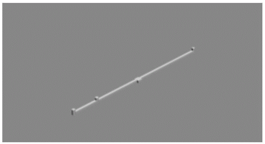
[0040] Step 1, using three-dimensional drawing software to design the microfluidic pipeline, the pipeline design is as follows: figure 1 As shown, the microfluidic channel lines are printed by fused deposition 3D, and the diameter range of the lines is 0.5-1mm, and the printed lines and filaments are cut into chip channels;

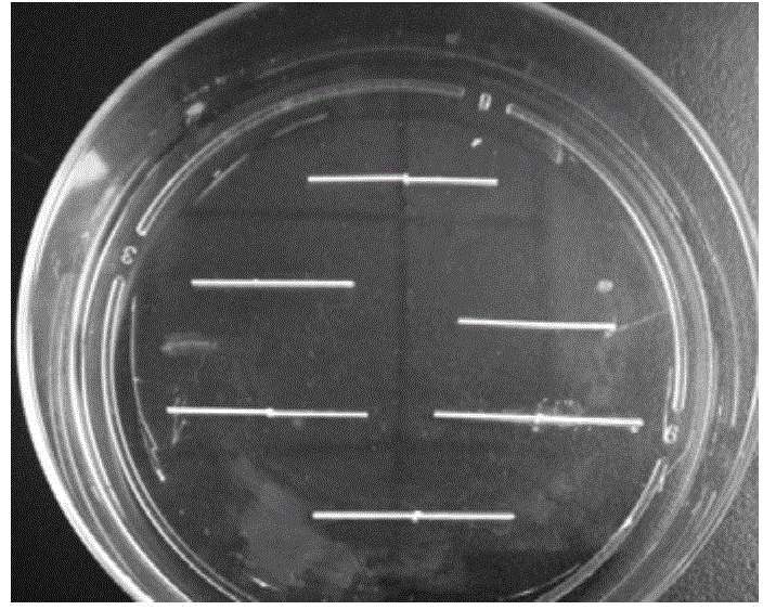
[0041] Step 2, then transfer to a watch glass, pass a little PDMS colloid, fix it on the substrate, such as figure 2 , pouring PDMS colloid in a surface dish, placing it in an 80-degree oven for 2 hours, curing and demoulding, drilling and bonding, and preparing a microfluidic chip;

[0042] The application of the microfluidic chip prepared above in surface-enhanced Raman detection specifically includes the following steps:

[0043] In the first step, the schematic diagram of the microfluidic chip pr...

Embodiment 2

[0052] This embodiment relates to a method for preparing a microfluidic chip based on 3D printing technology, the method comprising the following steps:

[0053] Step 1: Use 3D drawing software to design microfluidic pipelines, use fused deposition to 3D print microfluidic channel lines, the diameter of the lines ranges from 0.5 to 1mm, and cut the printed lines and filaments into chip channels;

[0054] Step 2, then transfer to a watch glass, pass a little PDMS colloid, fix it on the substrate, pour the PDMS colloid in the watch glass, place in a 60°C oven overnight, cure and demould, punch holes and bond, and prepare a microfluidic chip;

[0055] The application of the microfluidic chip prepared above in surface-enhanced Raman detection specifically includes the following steps:

[0056] In the first step, the monolithic column solution is injected into the microfluidic chip, and a point light source is used to expose the small cuboid area designed by the microfluidic chip t...

Embodiment 3

[0061] This embodiment relates to a method for preparing a microfluidic chip based on 3D printing technology, the method comprising the following steps:

[0062] Step 1: Use 3D drawing software to design microfluidic pipelines, use fused deposition to 3D print microfluidic channel lines, the diameter of the lines ranges from 0.1 to 1mm, and cut the printed lines and filaments into chip channels;

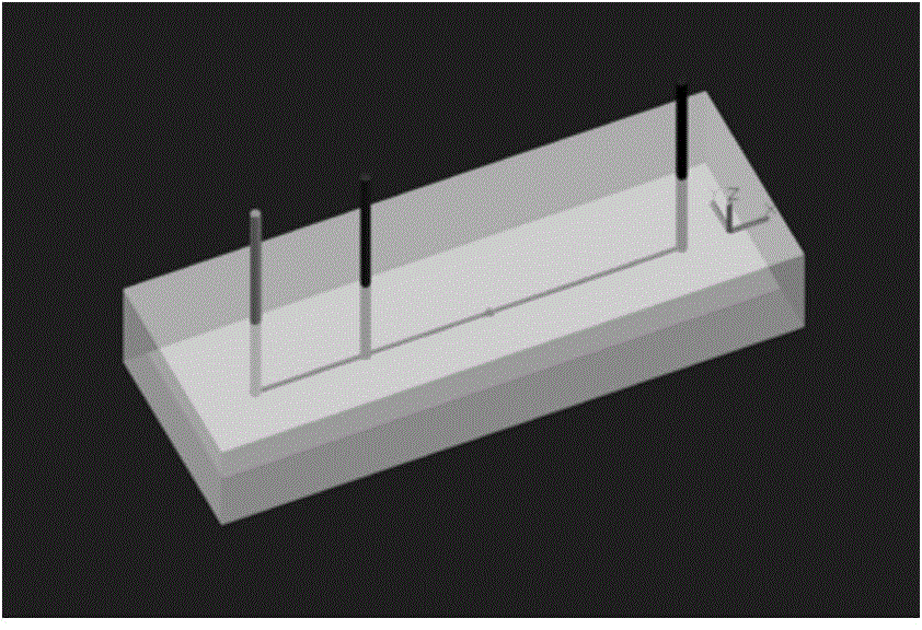
[0063] Step 2, then transfer to a watch glass, apply a small amount of 502 glue on the line, fix it to the substrate, pour PDMS colloid in the watch glass, place it in a 60°C oven for 6 hours, cure and demould, punch holes and bond, and prepare micro Fluidic chip, the schematic diagram of the microfluidic chip prepared based on 3D printing is as follows: image 3 shown.

[0064] The application of the microfluidic chip prepared above includes the following steps:

[0065] In the first step, the monolithic column solution is injected into the microfluidic chip, and a point light sou...


PUM


Abstract

The invention provides a preparation method and application of a micro-fluidic chip based on the 3D printing technique. The preparation method comprises the following steps: (1) designing a micro-fluidic pipeline, namely printing filament through a 3D desktop printer, wherein the filament is used as the channel mold plate of the micro-fluidic chip and made of acrylon-bivinyl-styrol copolymer, polylactic resin and vinol; (2) transferring the printed filament into a watch glass and fixing the filament on a substrate, then pouring PDMS colloid, curing, demolding, punching and bonding to prepare the micro-fluidic chip. The invention further relates to the application of the micro-fluidic chip in surface enhanced Raman detection. The preparation method is simple, rapid in processing and very cheap in cost, no complex micro-processing technique such as photo etching and developing is needed and the micro-fluidic chip can be prepared under a general experiment condition; the micro-fluidic chip is convenient to popularize and can be widely applied to the fields of human health, food safety, environment detection and medical diagnosis.

Description

technical field [0001] The invention relates to a preparation method of a microfluidic chip, in particular to a rapid preparation method of a microfluidic chip based on desktop 3D printing technology and its application. Background technique [0002] The microfluidic system is a micro-volume liquid (10 -9 –10 -18 L) The process of manipulation in pipes of tens to hundreds of microns, this technology has very broad application prospects in biomedicine, environmental monitoring, and food safety. Microfluidic devices have the following advantages, such as small size, reduced reagent consumption, and parallel detection of multiple samples. However, the preparation of traditional microfluidic chips requires complex processes such as mask plate preparation, glue removal, photolithography, and development. The preparation process is complex, the preparation cycle is long, the cost is high, and the processing technology is high. Finish. Contents of the invention [0003] In vi...

Claims


Application Information

Patent Timeline
Patent Type & Authority Applications(China)
IPC IPC(8): B01L3/00
Inventor 陈守慧施金豆叶磊丁显廷
Owner SHANGHAI JIAO TONG UNIV
Why Eureka
Try Eureka