

Method for cleaning bonding pads
A pad and cleaning solution technology, which is applied in electrical components, semiconductor/solid-state device manufacturing, circuits, etc., can solve the problems of wire bonding failure, poor pad tensile strength and joint strength uniformity, and easy corrosion of pads and other issues to achieve the effect of improving tensile strength and joint strength, optimizing electrical conductivity and reliability, and preventing corrosion
- Summary
- Abstract
- Description
- Claims
- Application Information
AI Technical Summary
Problems solved by technology
Method used
Image

Examples
Embodiment Construction
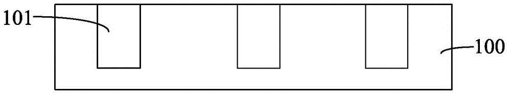
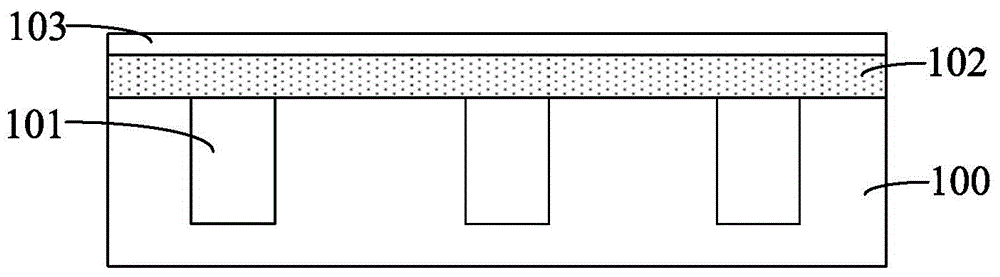
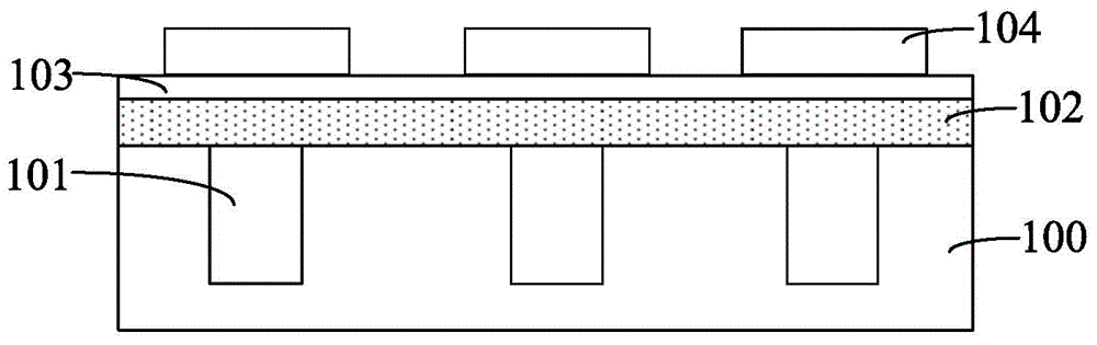
[0030] It can be seen from the background art that the quality of the pads formed in the prior art needs to be improved, resulting in the need to improve the conductivity and reliability of the semiconductor device.
[0031] According to the research on the causes of pad corrosion, it is found that after the pads are formed to realize the electrical connection between the inside of the chip and between the inside and the outside, the chip needs to be sliced (Die Saw). Deionized water is used to clean the chip. During the cleaning process, the pads on the chip are easily corroded, and corrosion pits (Corrosion Defect) appear on the surface of the pads, resulting in poor tensile strength and bonding strength of the pads; In the subsequent wire bonding process, when the pads with corrosion pits are connected to the package pins, due to the poor tensile strength and bonding strength of the pads, it is easy to cause wire bonding failure, which affects the conductivity and reliabil...
PUM
| Property | Measurement | Unit |
|---|---|---|
| thickness | aaaaa | aaaaa |
| thickness | aaaaa | aaaaa |
| thickness | aaaaa | aaaaa |
Abstract
Description
Claims
Application Information