Novel crystalline silicon cell wet process edge etching technology

A technology of crystalline silicon battery and wet method, which is applied in the direction of circuit, electrical components, sustainable manufacturing/processing, etc., can solve the problems of easy dripping of water, waste of acid, high leakage ratio, etc., to eliminate etching and save energy consumption Acid, cost reduction effect

Inactive Publication Date: 2015-09-09
RISEN ENERGY
View PDF3 Cites 5 Cited by
  • Summary
  • Abstract
  • Description
  • Claims
  • Application Information

AI Technical Summary

Problems solved by technology

[0005] 2) Schmid type: "water film" is used to protect the front, but because the silicon wafer is constantly moving, water is easy to drip into the etching tank to dilute the acid solution; in addition, because the outer layer of the silicon wafer is protected by PSG, a high concentration is required The acid can be carved through the edge; the final result is that this process wastes a lot of acid; the process see figure 2 shown
[0006] 3) Kutler type: first remove the PSG layer on the entire surface of the silicon wafer by spraying, and then cut the edge; since there is no protection of the PSG layer, this process will cause the p-n junction to be exposed to acid mist during edge cutting, Thereby destroying the p-n, causing the square resistance to increase
The parallel resistance of batteries made by this process is generally an order of magnitude lower than that of wet etching, which is not conducive to weak light effects, and the leakage ratio is relatively high

Method used


Image

  • Novel crystalline silicon cell wet process edge etching technology
  • Novel crystalline silicon cell wet process edge etching technology
  • Novel crystalline silicon cell wet process edge etching technology

Examples


Embodiment

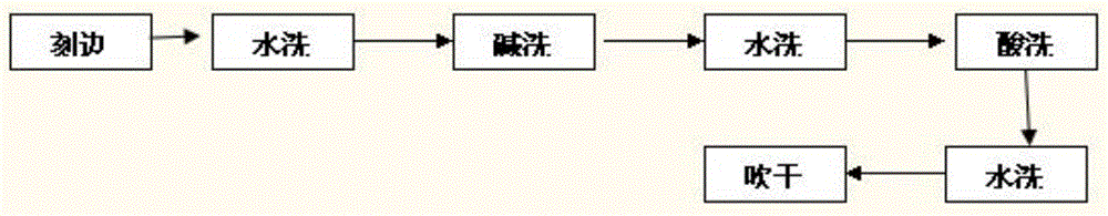
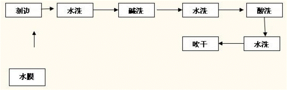
[0038] (1) Use HF to remove the PSG layer at the corner of the silicon wafer at room temperature by means of capillary roller carrying liquid or "floating on water"; the mass percentage concentration of HF is 3%, and the roller speed of the capillary roller is 2.5m / min;

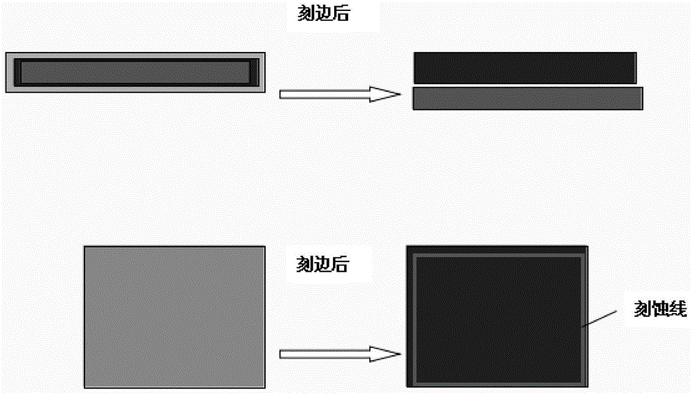
[0039] Principle: When HF removes the corner PSG, it will climb to the upper surface along the PSG layer, remove the PSG layer on the edge, and the surface of the silicon wafer after HF treatment is hydrophobic;

[0040] (2) dry the silicon chip surface after step (1) by air knife or hot air knife, the temperature of hot air knife is 60°-65°; the speed of roller is 2.5m / min;

[0041] (3) Use HF / HNO3 mixed acid to edge the silicon wafer dried in step (2) by means of capillary roller with liquid or "floating on water"; wherein the volume ratio of HF / HNO3 is 1:3, and the edge cutting speed is 2.4 m / min;

[0042] Principle: Since the edge of the PN junction layer of the silicon wafer treated with HF is hydrophob...


PUM


Abstract

The invention relates to a novel crystalline silicon cell wet process edge etching technology. The technology includes the following steps that: phosphosilicate glass (PSG) layers of edge corners of a silicon wafer are removed through utilizing HF; the concentration of mass percentage of the HF ranges from 2% to 5%; the treated surface of the silicon wafer is dried by hot air, and the temperature of the hot air ranges from 50 to 70 DEG C; edge etching is performed on the silicon wafer through utilizing mixed acid of HF and HNO3; the etched silicon wafer is washed in a water tank; the washed silicon wafer is arranged in an alkaline tank, so that porous silicon can be removed, and ammonium hydroxide of which the concentration of mass percentage ranges from 5% to 8% is adopted as alkali; and the silicon wafer which has been subjected to alkali treatment is arranged in the water tank so as to be washed; HF or mixed acid of HF/HCl, of which the mass percentage ranges from 2% to 5%, is utilized to remove the PSG; the volume ratio of the mixed acid of HF/HCl ranges from 1:2 to 4; the silicon wafer of which the PSG has been removed is arranged in the water tank so as to be washed; and the silicon wafer is dried by air. According to the novel crystalline silicon cell wet process edge etching technology of the invention, the PSG of the edge corners of the silicon wafer is removed at first innovatively, and therefore, chemical solutions can be prevented from climbing onto the front surface of the silicon wafer, and etching dents can be avoided.

Description

technical field [0001] The invention relates to the field of crystalline silicon solar cells, in particular to a novel wet edge engraving process for crystalline silicon cells. technical background. [0002] With the release of solar profit margins for crystalline silicon cells, the competition is getting bigger and bigger. How to reduce costs and improve the yield has become one of the important issues for every enterprise. After the silicon wafer is diffused, phosphorus will inevitably be diffused on the edge of the silicon wafer, and the photogenerated electrons collected on the front of the PN junction will diffuse to the back of the PN junction along the edge with phosphorus, causing a short circuit and reducing the parallel resistance. At the same time, due to the introduction of oxygen during the diffusion process, a layer of silicon dioxide is formed on the surface of the silicon wafer. At high temperatures, POCL3 and oxygen form P2O5, and some P atoms enter Si to re...

Claims


Application Information

Patent Timeline
Patent Type & Authority Applications(China)
IPC IPC(8): H01L31/18
CPCH01L31/18Y02P70/50
Inventor 张文锋陈波崔红星曾学仁
Owner RISEN ENERGY
Why Eureka
Try Eureka