

Nitride light-emitting diode structure and preparation method thereof
A technology of light-emitting diodes and nitrides, which is applied in the manufacture of semiconductor/solid-state devices, semiconductor devices, electrical components, etc., can solve the problems of slow cost reduction of LED devices, restrictions on the market penetration rate of LED devices, and difficulties in large-scale production. Ease of chip handling, reduction of lattice defects, and reduction of manufacturing costs
- Summary
- Abstract
- Description
- Claims
- Application Information
AI Technical Summary
Problems solved by technology
Method used
Image

Examples
Embodiment 1
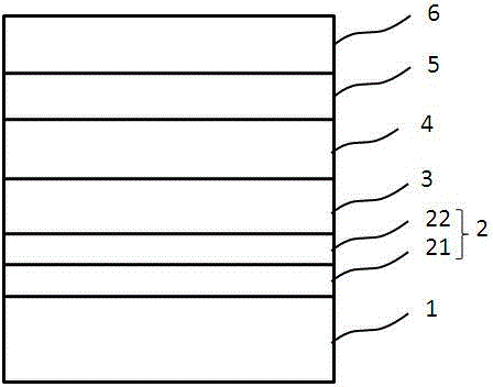
[0027] See attached figure 1 , provide a glass substrate 1, the glass substrate 1 is a patterned substrate or a non-patterned substrate, this embodiment is preferably a high temperature resistant (above 1300 ° C), patterned glass substrate; using MOCVD method on the glass substrate 1 The surface is sequentially epitaxially grown with a SiAlN layer 21 with a thickness of 15-300 angstroms and an AlGaN layer 22 with a thickness of 15-300 angstroms to form a buffer layer 2, a non-doped gallium nitride layer 3, an N-type GaN layer 4, and a quantum well structure Layer 5, P-type GaN layer 6. Wherein, the N-type GaN layer 4 can be selected from at least one of C, Si, Ge, Sn, Pb, O, S, Se, Te, Po as a dopant; the P-type GaN layer 6 can be selected from One of Be, Mg, Ca, Sr, and Ba is a dopant.
[0028] A method for preparing a nitride light-emitting diode provided by the present invention includes: providing a patterned glass substrate 1 resistant to high temperature (above 1300° C...
Embodiment 2
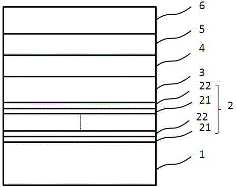
[0033] See attached figure 2 The difference between this embodiment and Embodiment 1 is that the buffer layer 2 is a cycle structure composed of a SiAlN layer 21 and an AlGaN layer 22, and its cycle number is 3. The specific method for growing the nitride light-emitting diode in this embodiment is as follows:
[0034] (1) Provide a high temperature resistant, patterned glass substrate;
[0035] (2) forming a SiAlN layer 21 on the surface of the substrate;
[0036] (3) Continue to grow the AlGaN layer 22 on the SiAlN layer 21 .
[0037] (4) Repeat steps (2) and (3) two more times.
[0038] (5) Continue to grow the non-doped gallium nitride layer 3 , the N-type GaN layer 4 , the quantum well structure layer 5 , and the P-type GaN layer 6 on the surface of the wafer after step (4).
[0039]Among them, since the material properties of the SiAlN layer 21 and the AlGaN layer 22 in the buffer layer structure 2 are sequentially close to those of the subsequent gallium nitride semi...
PUM
| Property | Measurement | Unit |
|---|---|---|
| thickness | aaaaa | aaaaa |
| temperature | aaaaa | aaaaa |
Abstract
Description
Claims
Application Information