Supercharge Your Innovation With Domain-Expert AI Agents!

Semiconductor device

A semiconductor and conductor layer technology, applied in the direction of semiconductor devices, semiconductor/solid-state device components, electric solid-state devices, etc., can solve the problems of increased cost, difficulty in adopting, and larger wiring and winding.

Active Publication Date: 2019-06-14
株式会社PANGEA
View PDF6 Cites 0 Cited by
  • Summary
  • Abstract
  • Description
  • Claims
  • Application Information

AI Technical Summary

Problems solved by technology

[0007] However, for example, if a memory chip and a controller chip are arranged on a narrow substrate, there may be cases in which restrictions on wiring routing become large, making it difficult to take countermeasures.
That is, there is a possibility that coplanar wiring cannot be used for a part of the data bus on the substrate
[0008] In order to increase the degree of freedom of wiring routing, it is also considered to increase the number of wiring layers on the substrate, but there is a concern that the cost will increase

Method used


Image

  • Semiconductor device
  • Semiconductor device
  • Semiconductor device

Examples


no. 1 Embodiment approach

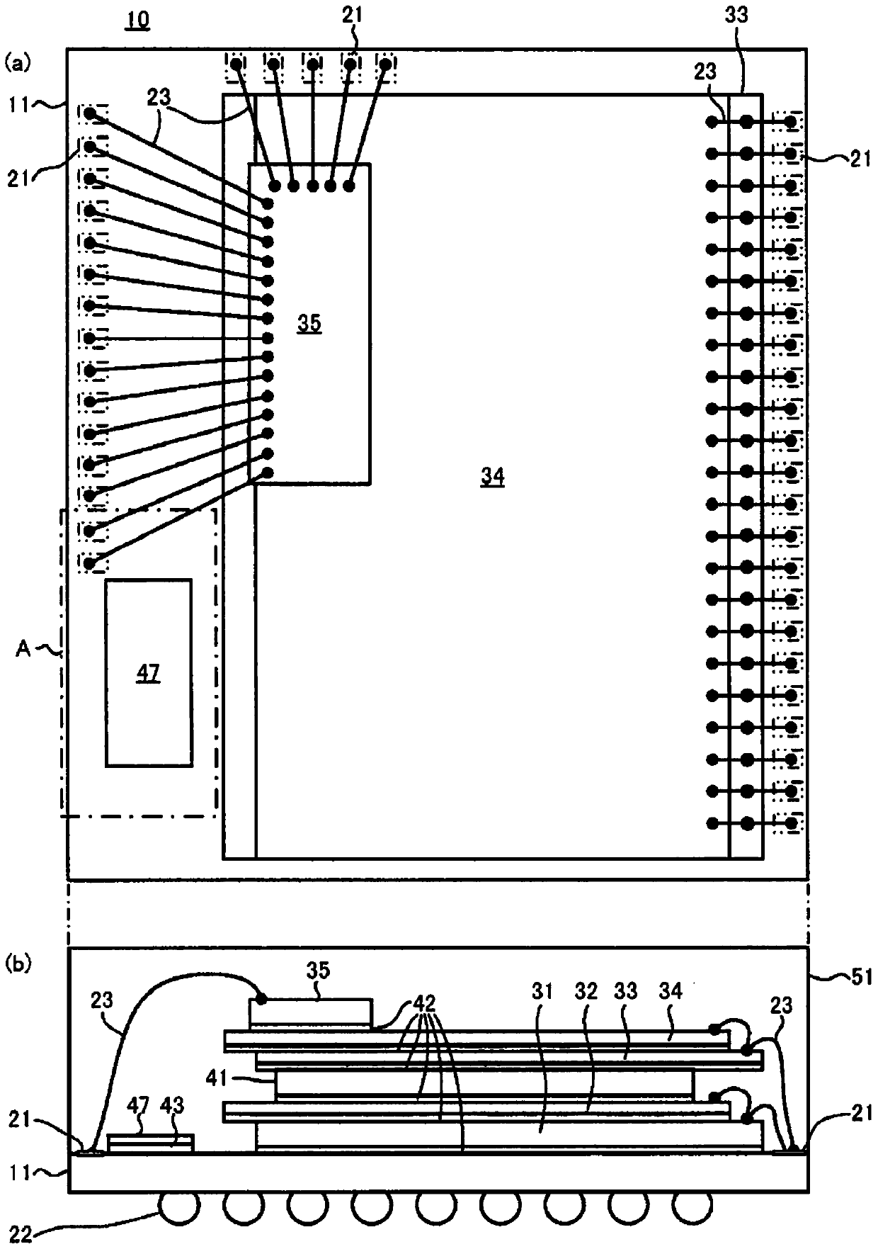
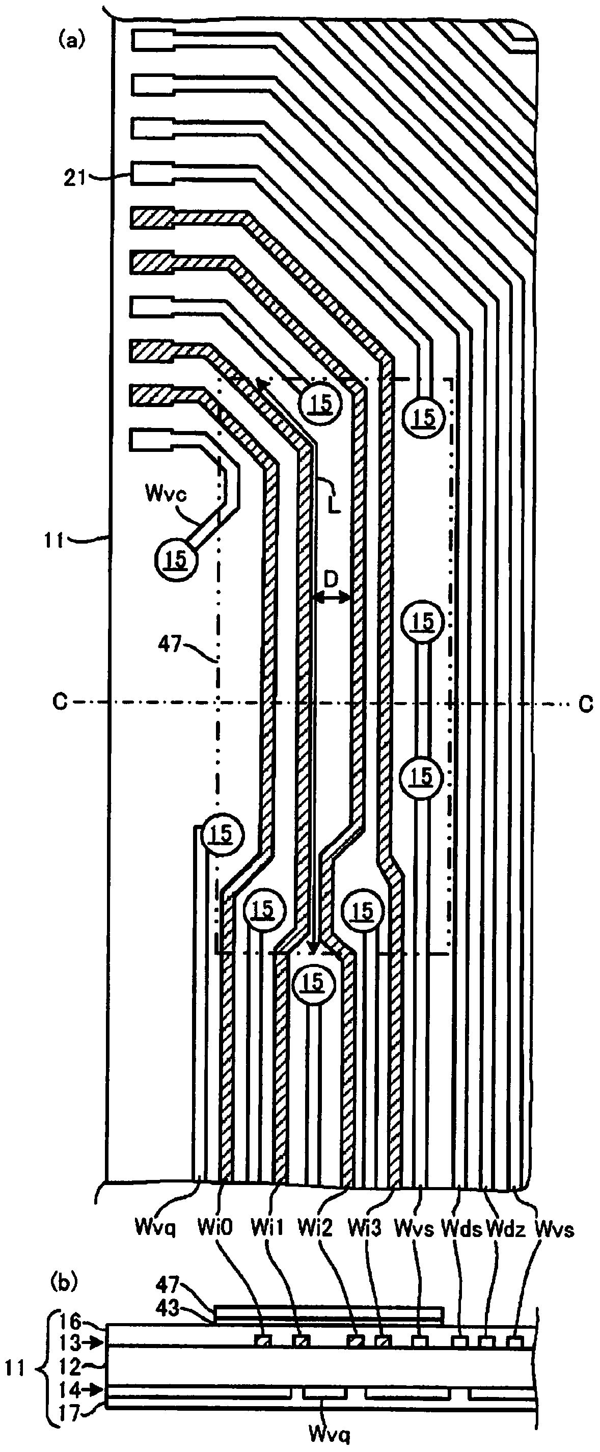
[0030] figure 1 (a) and (b) are respectively a plan view and a cross-sectional view of the semiconductor device 10 according to the first embodiment. figure 2 (a) and (b) are respectively figure 1 The enlarged top view and cross-sectional view of area A. figure 2 (b) means along figure 2 Section of line C-C of (a).

[0031] Furthermore, for ease of understanding, the figure 1 The description of wiring W is omitted in the figure 2 The description of the connection member 23 is omitted here. Moreover, hatching is attached|subjected to wiring Wi0-Wi3.

[0032] Such as figure 1 , figure 2 As shown, the semiconductor device 10 has a substrate 11 (core layer 12, wiring layers 13, 14, via holes 15, resist layers 16, 17), connection terminals 21, external terminals 22, connection members 23, memory chips 31-34 , a controller chip 35 , a spacer 41 , adhesive layers 42 , 43 , a conductor layer 47 , and a molding resin layer 51 .

[0033] The semiconductor device 10 is a s...

no. 2 Embodiment approach

[0084] Figure 5 (a) and (b) are respectively a plan view and a cross-sectional view of a semiconductor device 10a according to the second embodiment. Figure 6 (a) and (b) are respectively Figure 5 The enlarged top view and cross-sectional view of area A. Figure 6 (b) means along Figure 6 Section of line C-C of (a).

[0085] In this embodiment, the dummy chip 61 is arranged on the wiring layer 13 .

[0086] The dummy chip 61 has a silicon substrate 62 and a conductor layer 47 . In the present embodiment, the dummy chip 61 is mounted so that the conductor layer 47 faces the surface of the substrate 11 facing downward. The silicon substrate 62 in this embodiment functions as a semiconductor substrate arranged on the conductive layer 47 .

[0087] The conductor layer 47 has conductivity and paramagnetism, and the same material and thickness as the conductor layer 47 can be selected.

[0088] Also in this embodiment, as in the first embodiment, the conductive layer 47 r...

no. 3 Embodiment approach

[0090] Figure 7 (a) and (b) are respectively a plan view and a cross-sectional view of a semiconductor device 10b according to the third embodiment. Figure 8 (a) and (b) are respectively Figure 7 The enlarged top view and cross-sectional view of area A. Figure 8 (b) means along Figure 8 Section of line C-C of (a).

[0091] In the present embodiment, the dummy chip 61 is mounted face-up so that the conductive layer 47 side faces the opposite side of the substrate 11 . The silicon substrate 62 in this embodiment functions as a semiconductor substrate disposed between the conductive layer and the plurality of data signal lines.

[0092] Also in this embodiment, as in the first and second embodiments, the conductive layer 47 reduces the magnetic flux around the wirings Wi0 to Wi3, thereby reducing signal crosstalk.

[0093] As described above, in the above-described embodiment, by covering the region where the wirings Wi0 to Wi3 are adjacently arranged with the conductor...


PUM


Abstract

The invention provides a semiconductor device which can reduce wiring crosstalk on a substrate. The semiconductor device is provided with an insulation substrate, first and second semiconductor chips, a plurality of connectors, external terminals, a plurality of jointing elements, a plurality of data signal wires, and a conductor layer. The insulation substrate is provided with first and second main surfaces. The first semiconductor chip is configured on the first main surface. The second semiconductor chip is configured on the first semiconductor chip, and controls the first semiconductor chip. The plurality of connectors are configured on the first main surface. The external terminals are configured on the second main surface. The plurality of data signal wires have one end connected to any one of the plurality of connectors, the other end connected to the first semiconductor chip or the external terminal, and middle parts adjacent in a specific area of the first main surface. The conductor layer covers the specific area at intervals, and has electrical conductivity and paramagnetism.

Description

[0001] [Related applications] [0002] This application enjoys the priority of the basic application based on Japanese Patent Application No. 2014-52713 (filing date: March 14, 2014). This application incorporates all the contents of the basic application by referring to this basic application. technical field [0003] Embodiments of the present invention relate to a semiconductor device. Background technique [0004] There are cases where a memory chip (memory module) and a controller chip (control module) are stacked on a substrate and sealed with a mold resin to be used as a chip-laminated mold-sealed semiconductor package (hereinafter also referred to as "Packaging"). [0005] In this case, I / O (Input / Output) terminals of the memory chip are connected to external terminals of the package or I / O terminals of the controller chip via bonding wires or data bus lines (wiring) on ​​the substrate. Likewise, the I / O terminals of the controller chip are connected to the I / O te...

Claims


Application Information

Patent Timeline
Patent Type & Authority Patents(China)
IPC IPC(8): H01L23/31H01L23/498H01L25/16
CPCH01L2224/32145H01L2224/32225H01L2224/48091H01L2224/48145H01L2224/48147H01L2224/48227H01L2224/49171H01L2224/49175H01L2224/73265H01L2924/15311H01L2924/181H01L2924/00014H01L2924/00012H01L2924/00
Inventor 铃谷信人中村三昌尾山胜彦川村英树青木秀夫
Owner 株式会社PANGEA
Features
  • R&D
  • Intellectual Property
  • Life Sciences
  • Materials
  • Tech Scout
  • Unparalleled Data Quality
  • Higher Quality Content
  • 60% Fewer Hallucinations
Learn More