Preparation method of molybdenum disulfide thin film and molybdenum disulfide thin film
A molybdenum disulfide, thin film technology, applied in gaseous chemical plating, metal material coating process, coating and other directions, can solve the problems of poor film performance, poor film material compactness, and many sulfur vacancies, etc., to improve quality, fast The effect of transferring, reducing material defects
- Summary
- Abstract
- Description
- Claims
- Application Information
AI Technical Summary
Problems solved by technology
Method used
Image


Examples
specific Embodiment approach
[0014] The present invention provides a method for preparing a molybdenum disulfide thin film and the molybdenum disulfide thin film. In order to make the purpose, technical solution and effect of the present invention clearer and more definite, the present invention will be further described in detail below. It should be understood that the specific embodiments described here are only used to explain the present invention, not to limit the present invention.
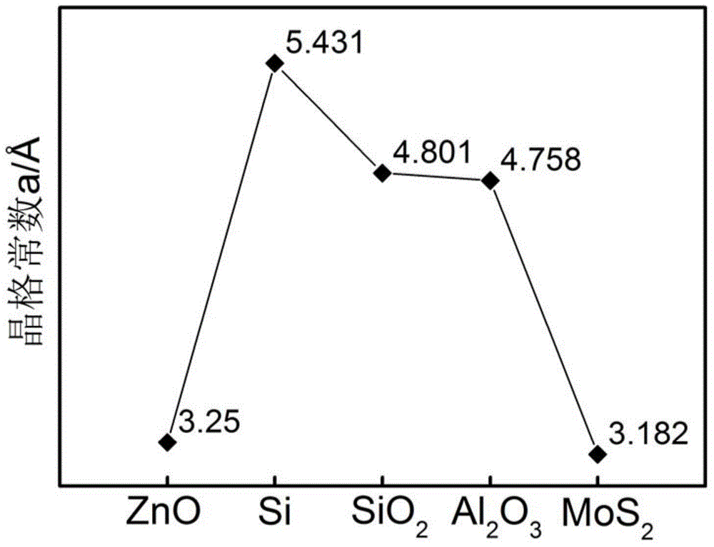
[0015] The preparation method of a kind of molybdenum disulfide film provided by the present invention uses chemical vapor deposition (CVD) to directly grow large-area, high-quality, low-defect molybdenum sulfide (MoS) on a silicon substrate coated with an oxide buffer layer. 2 ) film, and innovatively realize MoS 2 Rapid transfer of films.
[0016] At present, the main method to prepare large-area and high-quality molybdenum sulfide films is to use chemical vapor deposition (CVD) to deposit MoS 2 The growth of thin f...
Embodiment 1
[0037] One, the silicon (Si) substrate is cleaned, and the cleaning process includes the following steps:
[0038] 1. Ultrasonic cleaning of trichlorethylene;
[0039] 2. Acetone ultrasonic cleaning;
[0040] 3. Ethanol ultrasonic cleaning;
[0041] 4. Rinse in a beaker of deionized water;
[0042] 5. Sulfuric acid: nitric acid = 1:1, cook at 80°C for a few minutes, rinse with deionized water;
[0043] 6. Hydrochloric acid: hydrogen peroxide: water = 3:1:1, shake gently for a few minutes, rinse with deionized water;
[0044] 7. Hydrofluoric acid: water = 1:20, shake gently for a few minutes, rinse with deionized water;
[0045] 8. Rinse several times in a beaker of deionized water and rinse with running water.
[0046] 2. Use pulsed laser deposition (PLD) or magnetron sputtering technology and other similar technologies to coat a ZnO buffer layer on a silicon substrate with a thickness of about 130nm:
[0047] PLD technology is an ultra-high vacuum thin film preparation te...
PUM
| Property | Measurement | Unit |
|---|---|---|
| Thickness | aaaaa | aaaaa |
Abstract
Description
Claims
Application Information
 - R&D
- Intellectual Property
- Life Sciences
- Materials
- Tech Scout
- Unparalleled Data Quality
- Higher Quality Content
- 60% Fewer Hallucinations
Browse by: Latest US Patents, China's latest patents, Technical Efficacy Thesaurus, Application Domain, Technology Topic, Popular Technical Reports.
© 2025 PatSnap. All rights reserved.Legal|Privacy policy|Modern Slavery Act Transparency Statement|Sitemap|About US| Contact US: help@patsnap.com