Method for improving SiC and SiO2 interface state density

A technology of interface state density and S60, which is applied in the field of microelectronics, can solve the problems of low MOSFET channel mobility, ineffective H element passivation, and obstacles to the expected advantages of SiC devices, so as to improve mobility characteristics and reduce Interface state density, effect of improving interface quality

Active Publication Date: 2015-10-07
XIDIAN UNIV
View PDF2 Cites 10 Cited by
  • Summary
  • Abstract
  • Description
  • Claims
  • Application Information

AI Technical Summary

Problems solved by technology

Due to SiO 2 The high interface state of / SiC leads to the low mobility of the MOSFET channel, which seriously hinders the expected advantages of SiC devices.
Although improving SiO 2 The quality of the / SiC interface has been continuously improved, but the SiC / SiO 2 The interface state density is still higher than that of SiO 2 / Si interface states are an order of magnitude higher
For example, H and P elements are used to reduce the interface state density, but the passivation effect of H element is not obvious. Although P element can effectively reduce the interface state density, its realization process needs to be further improved.

Method used


Image

  • Method for improving SiC and SiO2 interface state density
  • Method for improving SiC and SiO2 interface state density
  • Method for improving SiC and SiO2 interface state density

Examples


Embodiment 1

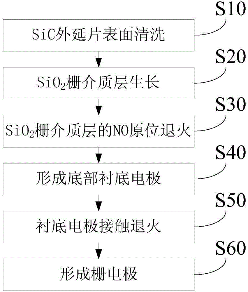
[0025] like figure 1 Shown, the embodiment of the present invention comprises the following steps:

[0026] S10. Cleaning the surface of the SiC epitaxial wafer by a standard cleaning method:

[0027] S101. Remove surface organic matter: immerse the SiC epitaxial wafer in acetone, trichlorethylene, acetone, methanol, and deionized water for 5 minutes each under ultrasonic conditions, and then use N 2 blow dry;

[0028] S102. Remove the intrinsic oxide layer on the surface: place the SiC epitaxial wafer after the first cleaning in HF acid solution for 15 minutes, and then oscillate with deionized water in ultrasonic waves for 5 minutes;

[0029] S103, placing the SiC epitaxial wafer cleaned for the second time in H 2 SO 4 :H 2 o 2 = 1:1 (volume ratio) soaked in the solution for 15min, H 2 SO 4 The concentration is 98%, H 2 o 2 The concentration is 27%, then rinse with deionized water;

[0030] S104, placing the SiC epitaxial wafer after the third cleaning in HF:H 2 ...

Embodiment 2

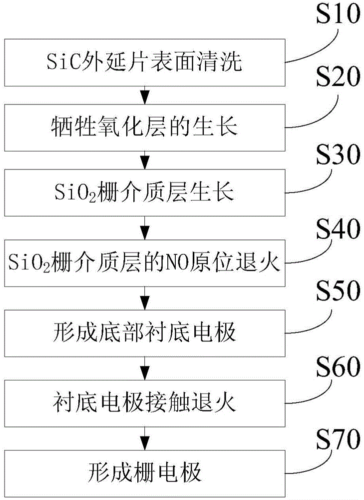
[0075] Compared with Example 1, in this example, on the basis of Example 1, SiO is grown in a large area 2 A sacrificial oxide growth process is added before the gate dielectric layer, which can effectively reduce the interface roughness and effectively improve the interface flatness.

[0076] like figure 2 As shown, this embodiment includes the following steps:

[0077] S10. Cleaning the surface of the SiC epitaxial wafer by a standard cleaning method:

[0078] S101. Remove surface organic matter: immerse the SiC epitaxial wafer in acetone, trichlorethylene, acetone, methanol, and deionized water for 5 minutes each under ultrasonic conditions, and then use N 2 blow dry;

[0079] S102. Remove the intrinsic oxide layer on the surface: place the SiC epitaxial wafer after the first cleaning in HF acid solution for 15 minutes, and then oscillate with deionized water in ultrasonic waves for 5 minutes;

[0080] S103, placing the SiC epitaxial wafer cleaned for the second time i...


PUM

PropertyMeasurementUnit
thicknessaaaaaaaaaa

Abstract

The invention provides a method for improving SiC and SiO2 interface state density and relates to the technical field of microelectronics. The method comprises: cleaning the surface of a SiC epitaxial wafer; growing a SiO2 gate dielectric layer; in-situ annealing the SiO2 gate dielectric layer by using NO gas; forming a bottom substrate electrode; contacting annealing the substrate electrode; and forming a gate electrode. The method anneals the SiO2 gate dielectric layer by using NO gas so as to reduce SiC / SiO2 interface state density and improve an interface, gate dielectric quality and device characteristics.

Description

technical field [0001] The invention relates to the technical field of microelectronics, in particular to an improved SiC and SiO 2 The interface state density method. Background technique [0002] SiC has unique physical, chemical and electrical properties, and is a semiconductor material with great development potential in extreme applications such as high temperature, high frequency, high power and radiation resistance. Due to SiO 2 The high interface state of / SiC leads to the low mobility of the MOSFET channel, which seriously hinders the expected advantages of SiC devices. Although improving SiO 2 The quality of the / SiC interface has been continuously improved, but the SiC / SiO 2 The interface state density is still higher than that of SiO 2 / Si interface states are an order of magnitude higher. For example, H and P elements are used to reduce the interface state density, but the passivation effect of H element is not obvious. Although P element can effectively r...

Claims


Application Information

Patent Timeline
Patent Type & Authority Applications(China)
IPC IPC(8): H01L21/04H01L21/02
CPCH01L21/02332H01L21/02337H01L21/049
Inventor 刘莉杨银堂
Owner XIDIAN UNIV
Why Eureka
Try Eureka