
Manufacture method of MEMS device

A manufacturing method and device technology, applied in the manufacture of microstructure devices, techniques for producing decorative surface effects, decorative art, etc., can solve the problem of the critical size of the opening 1, the sidewall of the opening 1 is not ideal, and the yield rate is difficult to obtain, etc. problems, to avoid surface roughness, smooth side walls, and improve yield

Inactive Publication Date: 2015-10-14
SHANGHAI HUAHONG GRACE SEMICON MFG CORP
View PDF5 Cites 1 Cited by
  • Summary
  • Abstract
  • Description
  • Claims
  • Application Information

AI Technical Summary

Problems solved by technology

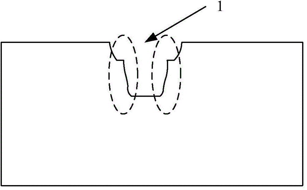
Depend on figure 1 It can be seen that the side wall of opening 1 is not ideal and is relatively rough, which also affects the critical dimension of opening 1
Therefore, it is difficult to obtain a better yield rate for the MEMS device structure made by the existing technology

Method used


Image

  • Manufacture method of MEMS device
  • Manufacture method of MEMS device
  • Manufacture method of MEMS device

Examples


Embodiment Construction

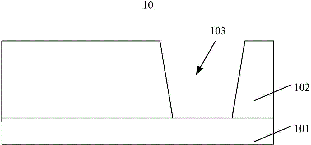
[0032] The manufacturing method of MEMS device of the present invention will be described in more detail below in conjunction with schematic diagram, wherein represents preferred embodiment of the present invention, should be appreciated that those skilled in the art can revise the present invention described here, and still realize the advantage of the present invention Effect. Therefore, the following description should be understood as the broad knowledge of those skilled in the art, but not as a limitation of the present invention.

[0033] In the interest of clarity, not all features of an actual implementation are described. In the following description, well-known functions and constructions are not described in detail since they would obscure the invention with unnecessary detail. It should be appreciated that in the development of any actual embodiment, numerous implementation details must be worked out to achieve the developer's specific goals, such as changing from...


PUM


Abstract

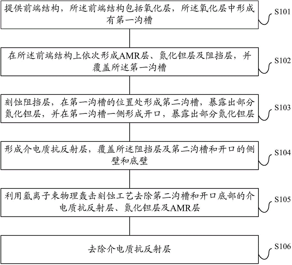
The invention discloses a manufacture method of MEMS device. The method comprises the steps as follows: providing a front end structure, wherein the front end structure comprises an oxide layer and a first groove is formed in the oxide layer; forming an AMR layer, a tantalum nitride layer and barrier layer on the front end structure in turn and covering the first groove; etching the barrier layer, forming a second groove at the place of the first groove to expose partial tantalum nitride layer, forming an opening at one side of the first groove to expose partial tantalum nitride layer; forming an dielectric substance anti-reflection layer to cover the barrier layer, the second groove and the side wall and bottom wall of the opening; using argon ion beam to physical sputter etching process to remove the dielectric substance anti-reflection layer, the tantalum nitride layer and the AMR layer located at the bottoms of the second groove and the opening; removing the dielectric substance anti-reflection layer. The manufacture method of the invention could well protect the side wall of the opening while etching via the dielectric substance anti-reflection layer so as to avoid the bombardment of the ion to the side wall of the opening to ensure the key size of the opening, thereby improving the yield rate of the product.

Description

technical field [0001] The invention relates to the technical field of semiconductors, in particular to a manufacturing method of a MEMS device. Background technique [0002] In recent years, with the development of micro-electromechanical system (Micro-Electrico-Mechanical-System, MEMS) technology, various micro-electromechanical devices, including: micro-sensors, micro-actuators, etc., have achieved miniaturization, which is beneficial to Improve device integration, so MEMS has become one of the main development directions. [0003] Nowadays, microelectromechanical systems manufactured using anisotropic magnet resistive (AMR) have the characteristics of high sensitivity, good thermal stability, low material cost, and simple preparation process, and have been widely used. [0004] The manufacturing process of MEMS devices in the prior art mainly includes: [0005] Step S1, providing a front-end structure, specifically including a substrate and an oxide layer on the substr...

Claims


Application Information

Patent Timeline
IPC IPC(8): B81C1/00
Inventor 张振兴
Owner SHANGHAI HUAHONG GRACE SEMICON MFG CORP
Learn More