

Method for forming semiconductor device
A semiconductor and device technology, applied in the field of semiconductor device formation, can solve the problems of shrinking the size of fin field effect transistors, increasing the difficulty of the fin field effect transistor process, increasing device density, etc., and achieves good appearance and simplified formation method. , size-accurate effect
- Summary
- Abstract
- Description
- Claims
- Application Information
AI Technical Summary
Problems solved by technology
Method used
Image

Examples
Embodiment Construction
[0035] As mentioned in the background art, with the shrinking of the process node, the size of the FinFET is reduced and the device density is increased, so that the process difficulty of forming the FinFET continues to increase.
[0036] After research, it is found that as the process node shrinks, the space for forming the conductive structure on the surface of the source region, the drain region or the gate layer also shrinks, making it more difficult to form the conductive structure, and the formed conductive structure The appearance is poor.
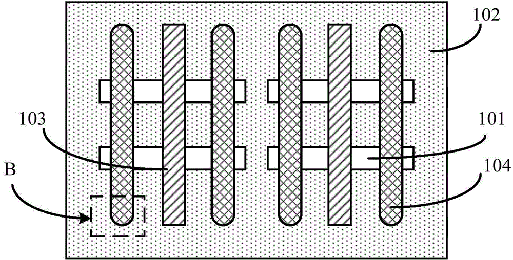
[0037] For details, please refer to figure 1 , figure 1 It is a top-view structural diagram of a fin field effect transistor, including: a substrate (not shown); several parallel fins 101 arranged in an array on the surface of the substrate; The dielectric layer 102 of the wall; the gate structure 103 across the fin 101 and the dielectric layer 102, the source region and the drain region (not shown) in the fin 101 on both sides of...
PUM
 Abstract
Description
Claims
Application Information