Multi-junction GaAs thin-film solar cell based on forward mismatched epitaxial growth

A solar cell and battery technology, applied in the field of solar cells, can solve the problems of expensive preparation of GaAs thin-film solar cells, etc., and achieve the effects of improving photoelectric conversion efficiency, improving application prospects, and high connection mechanical strength

Inactive Publication Date: 2015-10-21
CHINA ELECTRONIC TECH GRP CORP NO 18 RES INST
View PDF4 Cites 5 Cited by
  • Summary
  • Abstract
  • Description
  • Claims
  • Application Information

AI Technical Summary

Problems solved by technology

[0011] Nowadays, most of the manufacturing process of GaAs thin film solar cells adopts the thin film cell process of directly etching away the growth substrate to realize the transfer of epitaxial thin film layer, which makes the preparation cost of GaAs thin film solar cells quite expensive

Method used


Image

  • Multi-junction GaAs thin-film solar cell based on forward mismatched epitaxial growth
  • Multi-junction GaAs thin-film solar cell based on forward mismatched epitaxial growth
  • Multi-junction GaAs thin-film solar cell based on forward mismatched epitaxial growth

Examples


Embodiment Construction

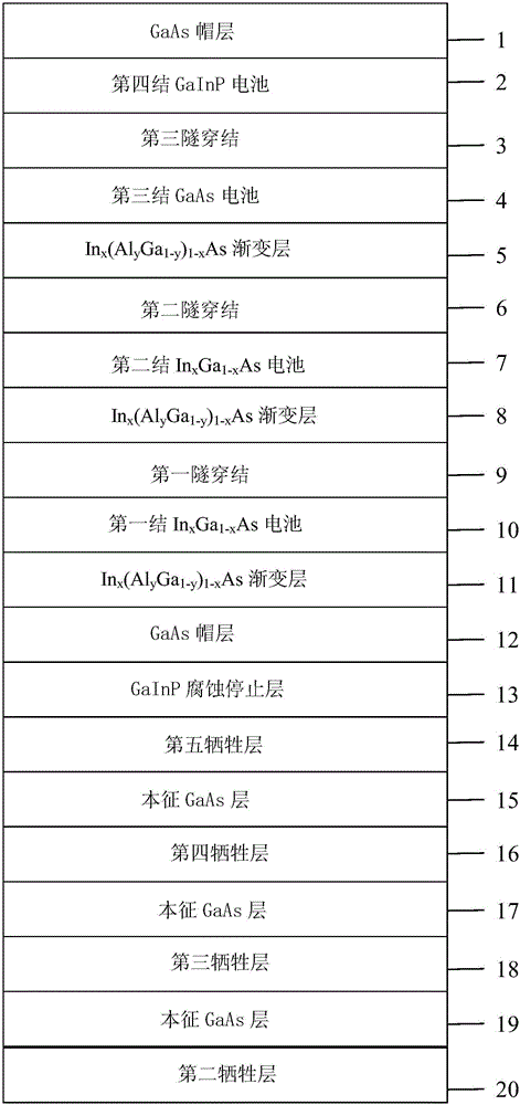
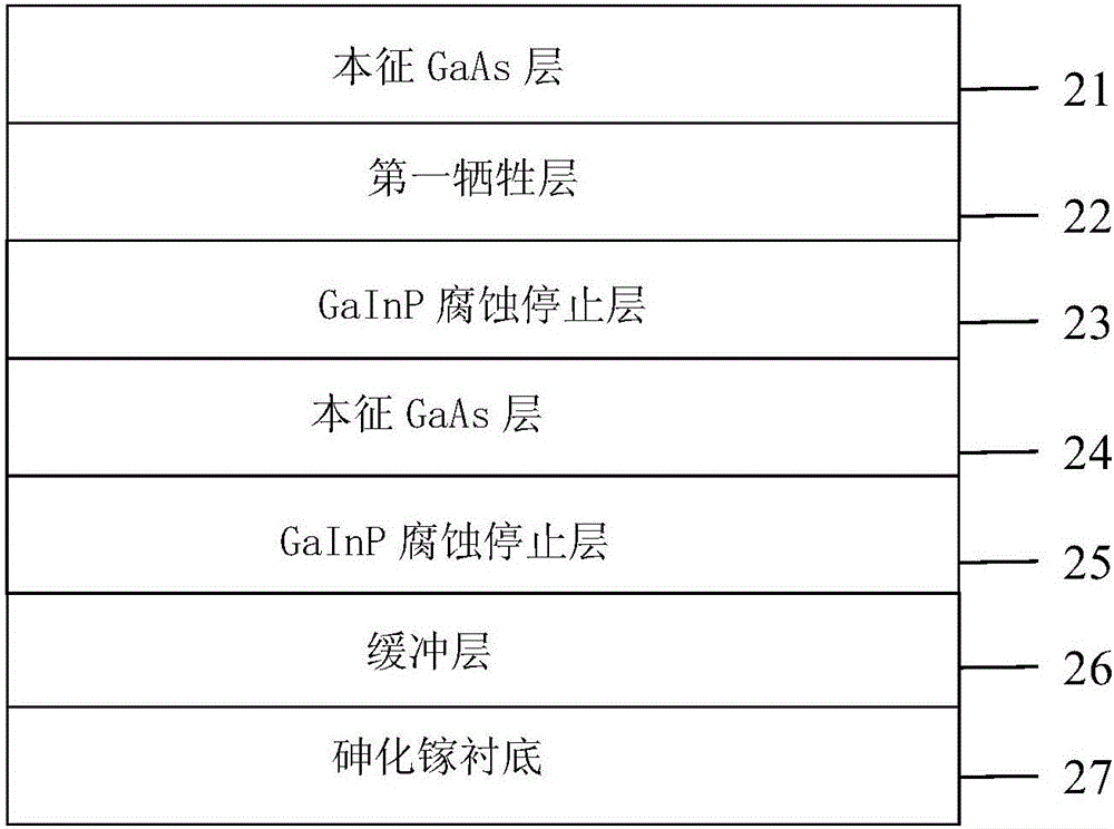
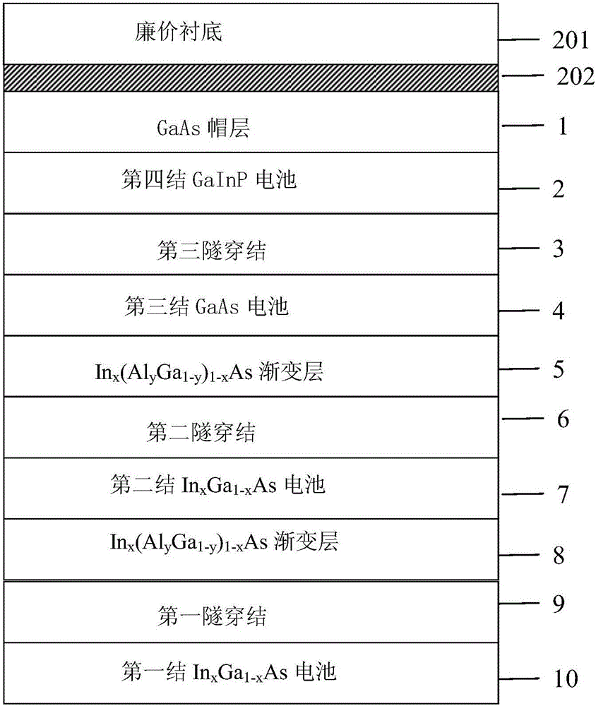
[0040] This embodiment provides a GaAs four-junction thin-film solar cell based on epitaxial forward mismatch growth. Firstly, a structure combining the cell body and the active layer of the cell is prepared, including a gallium arsenide substrate, a buffer layer, a GaInP corrosion stop layer, and this Intrinsic GaAs layer, GaInP etch stop layer, first sacrificial layer, intrinsic GaAs layer, second sacrificial layer, intrinsic GaAs layer, third sacrificial layer, intrinsic GaAs layer, fourth sacrificial layer, intrinsic GaAs layer, second sacrificial layer Five sacrificial layers, GaInP etch stop layer, GaAs cap layer, In x (Al y Ga 1-y ) 1-x As gradient layer, first junction In x Ga 1-x As cell, first tunnel junction, In x (Al y Ga 1-y ) 1-x As gradient layer, second junction In x Ga 1-x As cell, second tunnel junction, In x (Al y Ga 1-y ) 1-x As graded layer, third junction GaAs cell, third tunnel junction, fourth junction GaInP cell, GaAs capping layer.

[0...


PUM


Abstract

The invention belongs to the field of solar cells and particularly relates to a multi-junction GaAs thin-film solar cell based on forward mismatched epitaxial growth. The solar cell comprises a GaAs cap layer, an In<x>(Al<y>Ga<1-y>)<1-c>As gradually-changing layer, a first knot In<x>Ga<1-x>As cell, a first tunnel junction knot, an In<x>(Al<y>Ga<1-y>)<1-x>As gradually-changing layer, a second knot In<x>Ga<1-x>As cell, a second tunnel junction knot, an In<x>(Al<y>Ga<1-y>)<1-c>As gradually-changing layer, a third GaAs cell, a third tunnel junction knot, a fourth knot GaInP cell, and a GaAs cap layer. The solar cell is prepared by using the forward mismatched epitaxial growth technology and the corroded substrate stripping technology. The stripped GaAs substrate can be reused for the epitaxial growth of the solar cell by the chemical-mechanical polishing, and cleaning technology, thereby achieving reuse of the GaAs substrate. Via the forward epitaxial growth technology, micro-area defects alternatively generated and controlled via lattice mismatching are gradually annihilated or extend toward edges, thereby ensuring well epitaxial growth of the cell and further improving photoelectric conversion efficiency of the solar cell.

Description

technical field [0001] The invention relates to the field of solar cells, in particular to a multi-junction GaAs thin film solar cell. Background technique [0002] At present, in the photovoltaic market, thin-film solar cells of various materials occupy a place in the photovoltaic market with their unique advantages and gradually mature technology, and their growth rate is very fast. [0003] The product types of thin-film solar cells mainly include CdTe thin-film batteries, silicon-based thin-film batteries and copper indium gallium tin (CIGS) thin-film batteries. Compared with conventional crystalline silicon solar cells, the above-mentioned thin-film batteries use less materials, and the thickness of the thin-film materials constituting the solar cells does not exceed 50 microns, while the thickness of crystalline silicon cells is about 180-200 microns. In addition, thin-film solar cells have attracted much attention because of their cheap substrate materials (such as g...

Claims


Application Information

Patent Timeline
IPC IPC(8): H01L31/0725H01L31/0735H01L31/18
CPCH01L31/0725H01L31/0735H01L31/1844H01L31/1896Y02E10/544Y02P70/50
Inventor 高鹏孙强肖志斌刘如彬薛超张启明
Owner CHINA ELECTRONIC TECH GRP CORP NO 18 RES INST
Why Eureka
Try Eureka