Light-emitting diode epitaxial wafer

A technology of light-emitting diodes and epitaxial wafers, which is applied to electrical components, circuits, semiconductor devices, etc., can solve the problems of low quantum efficiency in epitaxial wafers, and achieve the effects of increasing internal quantum efficiency, improving injection efficiency, and increasing luminous efficiency

Active Publication Date: 2015-10-21
HC SEMITEK SUZHOU
View PDF5 Cites 9 Cited by
  • Summary
  • Abstract
  • Description
  • Claims
  • Application Information

AI Technical Summary

Problems solved by technology

[0005] In order to solve the problem of low internal quantum efficiency of existing epitaxial wafers, an embodiment of the present invention provides a light-emitting diode epitaxial wafer

Method used


Image

  • Light-emitting diode epitaxial wafer
  • Light-emitting diode epitaxial wafer
  • Light-emitting diode epitaxial wafer

Examples


Embodiment

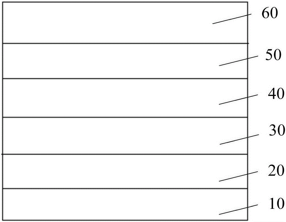
[0031] An embodiment of the present invention provides a light emitting diode epitaxial wafer, see figure 1 , the epitaxial wafer includes: a substrate 10 , a buffer layer 20 , an undoped GaN layer 30 , an N-type layer 40 , a multi-quantum well layer 50 , and a P-type layer 60 sequentially covering the substrate 10 .

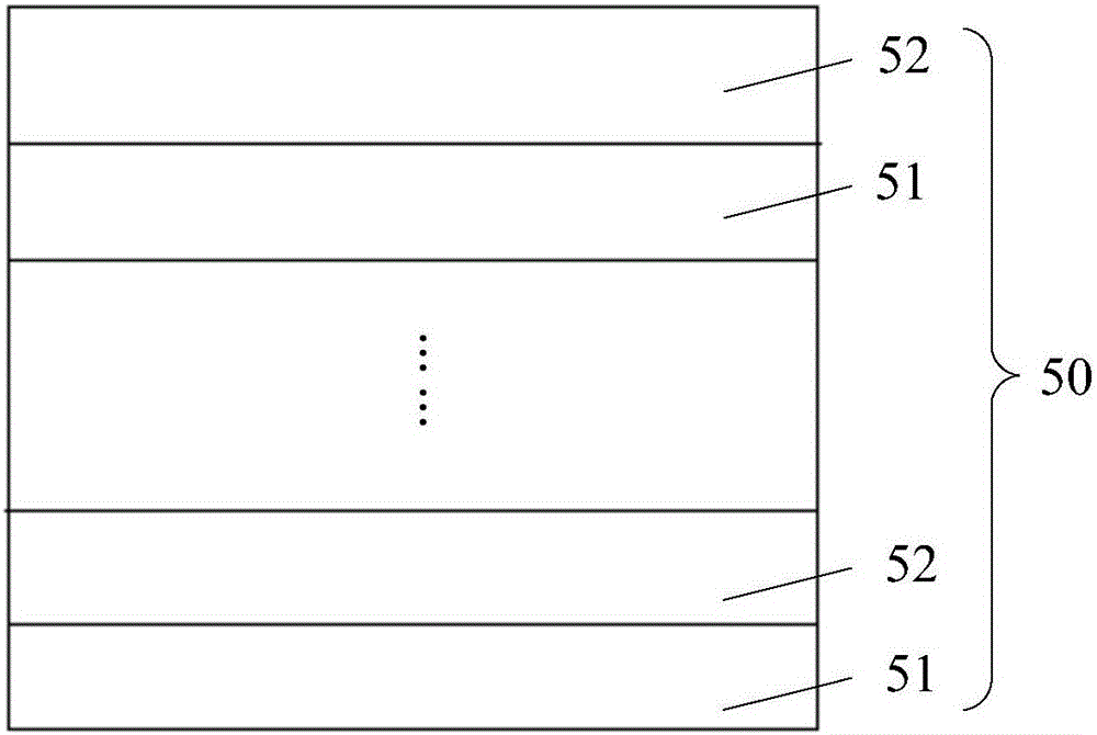
[0032] see figure 2 , the multi-quantum well layer 50 is a multi-period structure, and each periodic structure includes: a quantum well layer 51 and a quantum barrier layer 52 covering the quantum well layer 51, and the quantum barrier layer 52 closest to the P-type layer 60 is a supercrystalline grid structure.

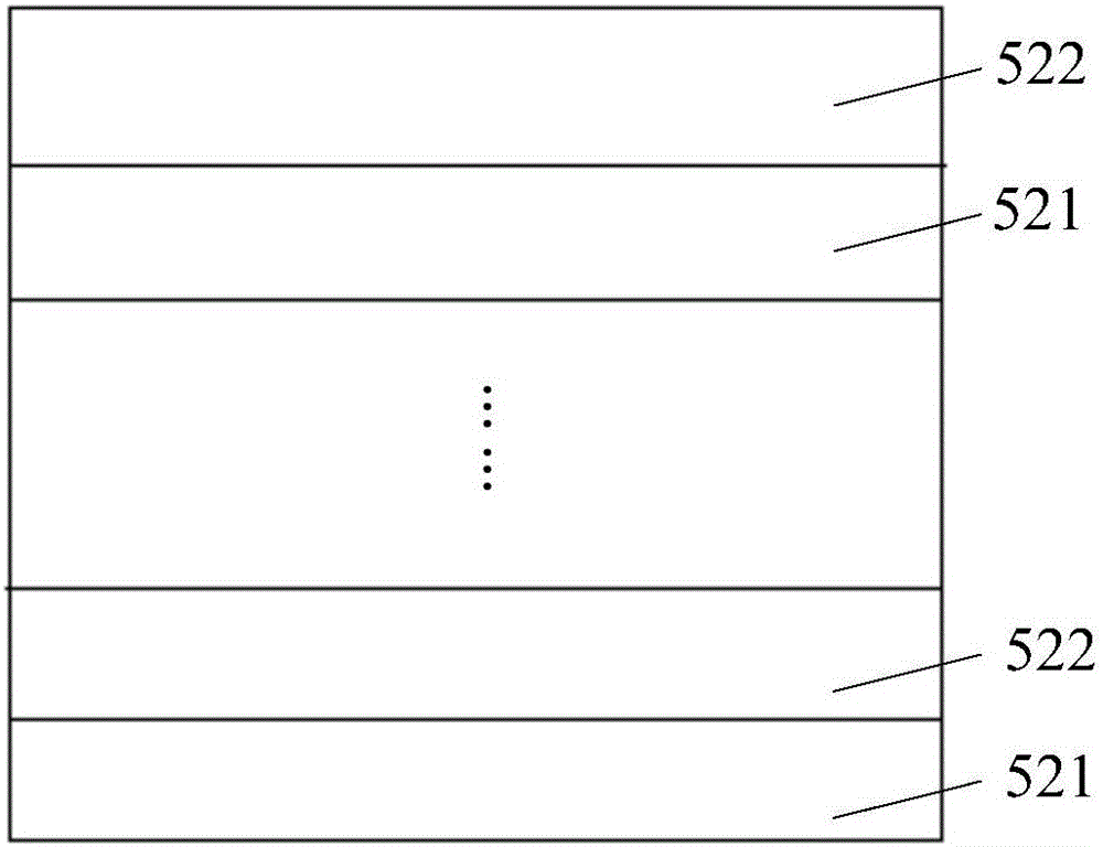
[0033] see image 3 , the superlattice structure includes: a plurality of alternately grown Al x Ga 1-x N sublayer 521 and GaN sublayer 522, 0x Ga 1-x The composition of Al in the N sublayer 511 changes gradually with the growth sequence.

[0034] In this embodiment, the substrate 10 may be a sapphire substrate, or a Si substrate or a SiC substr...


PUM


Abstract

The invention discloses a light-emitting diode epitaxial wafer and belongs to the technical field of semiconductors. The epitaxial wafer comprises a substrate, and a buffer layer, a non-impurity-doped GaN layer, an N-type layer, a multi-quantum well layer and a P-type layer which successively cover the substrate. The multi-quantum well layer is of a multi-period structure, and each period structure comprises a quantum well layer and a quantum barrier layer covering the quantum well layer. The quantum barrier layer closest to the P-type layer is of a superlattice structure. The superlattice structure comprises a plurality of AlxGal-xN sub-layers and GaN sub-layers which grow in an alternating manner, wherein x is larger than zero and less than 1, and the components of Al in the AlxGal-xN sub-layers gradually changes with the growth sequence. According to the invention, the quantum barrier layer, closest to the P-type layer, in the multi-quantum well layer of the epitaxial wafer is set as the superlattice structure, electronic overflow is effectively prevented on one hand, and on the other hand, the cavity injection rate is increased, so that the internal quantum efficiency of the epitaxial wafer is further increased, and the light-emitting efficiency of the light-emitting diode is improved.

Description

technical field [0001] The invention relates to the technical field of semiconductors, in particular to a light-emitting diode epitaxial wafer. Background technique [0002] Light Emitting Diodes ("LED" for short) are semiconductor electronic components that can convert electrical energy into light energy. [0003] In the conventional preparation method of light-emitting diode epitaxial wafers, metal-organic chemical vapor deposition (Metal-organic Chemical Vapor Deposition, referred to as "MOCVD") method is used to deposit A buffer layer, an undoped GaN layer, an N-type layer, a multi-quantum well layer, and a P-type layer are grown sequentially. [0004] In the existing light-emitting diode epitaxial wafer, on the one hand, there is electron overflow in the multi-quantum well layer, and the overflowed electrons enter the P-type layer and undergo non-radiative recombination with the holes in the P-type layer; on the other hand, the P-type The holes in the multi-quantum we...

Claims


Application Information

Patent Timeline
Patent Type & Authority Applications(China)
IPC IPC(8): H01L33/06H01L33/32H01L33/00
CPCH01L33/0066H01L33/0075H01L33/06H01L33/325
Inventor 李昱桦乔楠陈柏松胡加辉魏世祯
Owner HC SEMITEK SUZHOU
Why Eureka
Try Eureka