Super-junction semiconductor device and manufacture method thereof

A super-junction semiconductor and manufacturing method technology, which is applied in the direction of semiconductor/solid-state device manufacturing, semiconductor devices, transistors, etc., can solve the problems of surface MOS structure shrinkage, on-resistance increase, and large process difficulty, so as to reduce process difficulty and manufacture cost, alleviate the dv/dt is too large, increase the effect of the current flow path

Inactive Publication Date: 2015-10-28
WUXI NCE POWER
View PDF9 Cites 5 Cited by
  • Summary
  • Abstract
  • Description
  • Claims
  • Application Information

AI Technical Summary

Problems solved by technology

Such shrinkage will bring many problems, such as the increase in the benefits of JFET in the adjacent P-type body area, and the on-resistance (Rdson) of the device cannot be further reduced under the same withstand voltage requirements; the surface MOS caused by the reduction in the size of the super-junction structure unit The structure shrinks or even fails to meet the manufacturing requirements
Chinese Patent ZL 201080021229.3 Although the disclosed super-junction structure can solve the contradiction between the size reduction of the super-junction structure unit and the surface MOS structure, because the P-pillar under the gate occupies the key JFET area, the on-resistance of the actual product will increase significantly
A trench with a larger aspect ratio faces greater process difficulties in etching and epitaxial filling. When the depth of a deep trench is more than 35 μm and the width is less than 3 μm, existing equipment and manufacturing processes face great challenges
In the traditional manufacturing method of multiple photolithography, implantation, and epitaxy, due to the thermal process of multiple epitaxy, the width of the P-type column in the drift region is difficult to achieve a smaller size.

Method used


Image

  • Super-junction semiconductor device and manufacture method thereof
  • Super-junction semiconductor device and manufacture method thereof
  • Super-junction semiconductor device and manufacture method thereof

Examples


Embodiment Construction

[0047] The present invention will be further described below in conjunction with specific drawings and embodiments.

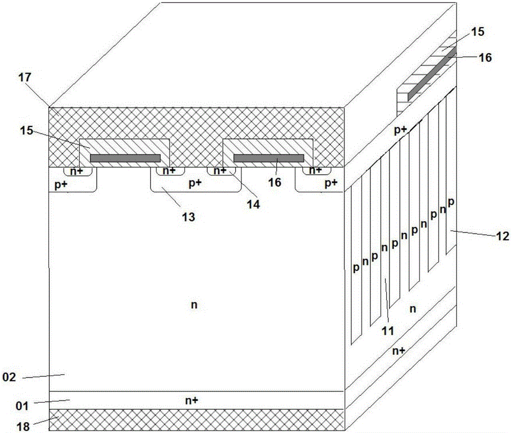
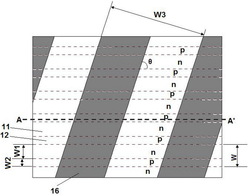
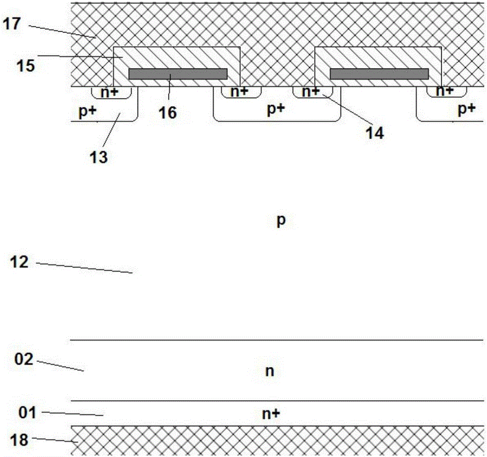
[0048] Such as figure 1 , figure 2 with image 3 As shown: taking an N-type planar superjunction vertical metal oxide field effect transistor as an example, the present invention includes a semiconductor substrate, and the semiconductor substrate includes an N-type substrate 01 and an N-type drift adjacent to the N-type substrate 01 Zone 02, the upper surface of the N-type drift zone 02 forms the first main surface of the semiconductor substrate, and the lower surface of the N-type substrate 01 forms the second main surface of the semiconductor substrate; A super junction structure formed by alternate arrangement of P columns 12, N columns 11 and P columns 12 in the super junction structure extend from the first main surface along the first main surface to the second main surface in the N-type drift region 02 Several device cells are set on the first main ...


PUM


Abstract

The invention relates to a super-junction semiconductor device and a manufacture method thereof. The pitch of the super-junction structure of the super-junction semiconductor device is W. The width of a first conductive type column in the super-junction structure is W1. The width of a second conductive type column in the super-junction structure is W2. The W=W1+W2. The pitch of a device cell is W3. Any second conductive type column in the super-junction structure is in contact with at least one second conductive type body region. The pitch W of the super-junction structure is less than the pitch W3 of the device cell. The width W1 of the first conductive type column in the super-junction structure is not less than the width W2 of the second conductive type column. The super-junction semiconductor device effectively solves a direct contradiction between a decrease in the pitch of the super-junction structure in a drift region and the device cell, further reduce device on-state resistance, has a better switching characteristic, and obviously decreases the pitch of the super-junction structure while process cost and process difficulty are not increased.

Description

technical field [0001] The invention relates to a semiconductor device and a manufacturing method, in particular to a super-junction semiconductor device and a manufacturing method thereof, belonging to the technical field of super-junction semiconductor devices. Background technique [0002] In the field of medium and high voltage power semiconductor devices, the super junction structure (Super Junction) has been widely used. Compared with traditional power MOSFET devices, the super junction structure can obtain a better compromise relationship between device withstand voltage and on-resistance. The super junction structure is formed in the drift region of the semiconductor device. The super junction structure formed in the drift region includes N-conductivity type pillars (N pillars) and P conductivity-type pillars (P pillars). The N pillars and P pillars are alternately adjacent to each other. A plurality of P-N column pairs form a super junction structure. The N column ...

Claims


Application Information

Patent Timeline
Patent Type & Authority Applications(China)
IPC IPC(8): H01L29/78H01L29/739H01L29/06H01L21/311H01L21/336
CPCH01L29/7802H01L29/0684H01L29/66333H01L29/66348H01L29/66712H01L29/66734H01L29/7395H01L29/7397H01L29/7813
Inventor 朱袁正李宗清
Owner WUXI NCE POWER
Why Eureka
Try Eureka