Low noise amplifier for MEMS capacitive transducers

A transducer and amplifier circuit technology, applied in low-noise amplifiers, electrostatic transducer microphones, low-frequency amplifiers, etc., can solve the problems of high power consumption, output signal distortion, low power, etc.

Active Publication Date: 2015-11-04
CIRRUS LOGIC INT SEMICON
View PDF5 Cites 25 Cited by
  • Summary
  • Abstract
  • Description
  • Claims
  • Application Information

AI Technical Summary

Problems solved by technology

However, this example is not ideal and wastes power in distorting electrical linearity
Furthermore, the signal component of the current delivered to the current connected to the output load impedance of the amplifier is provided by a similar modulation of the current flowing through the MOS transistor, resulting in a signal dependent change in the gate-source voltage of the MOS transistor
This produces a load-dependent attenuation of the output signal, which also becomes significantly non-linear for large output signal swings, resulting in distortion of the output signal
In other words, the non-zero output impedance of the source follower produces a load-dependent gain and the signal dependence of this output impedance introduces distortion of the large output signal
The output impedance can be reduced by using a higher bias current, but this causes undesirably higher power dissipation
[0005] Although simpler and lower power than amplifiers that include differential input stages, conventional source follower amplifiers have an inherent fixed gain close to 1 or less

Method used


Image

  • Low noise amplifier for MEMS capacitive transducers
  • Low noise amplifier for MEMS capacitive transducers
  • Low noise amplifier for MEMS capacitive transducers

Examples


Embodiment Construction

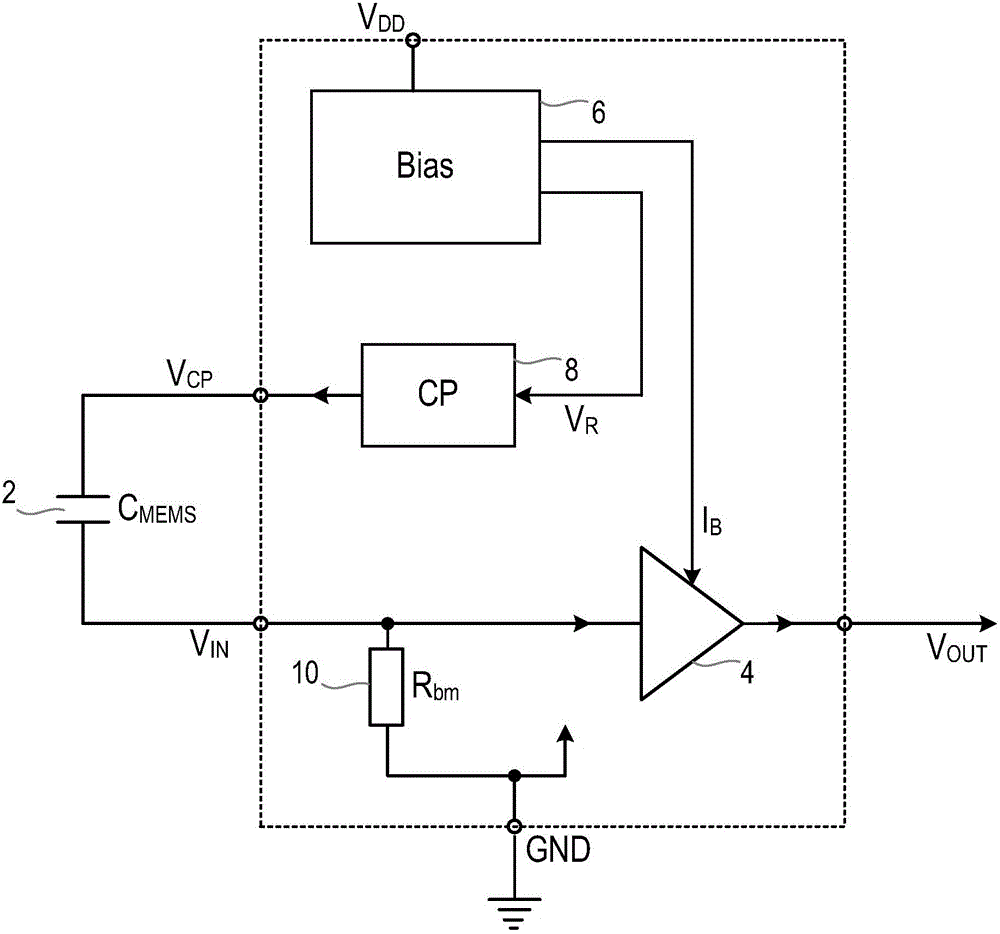
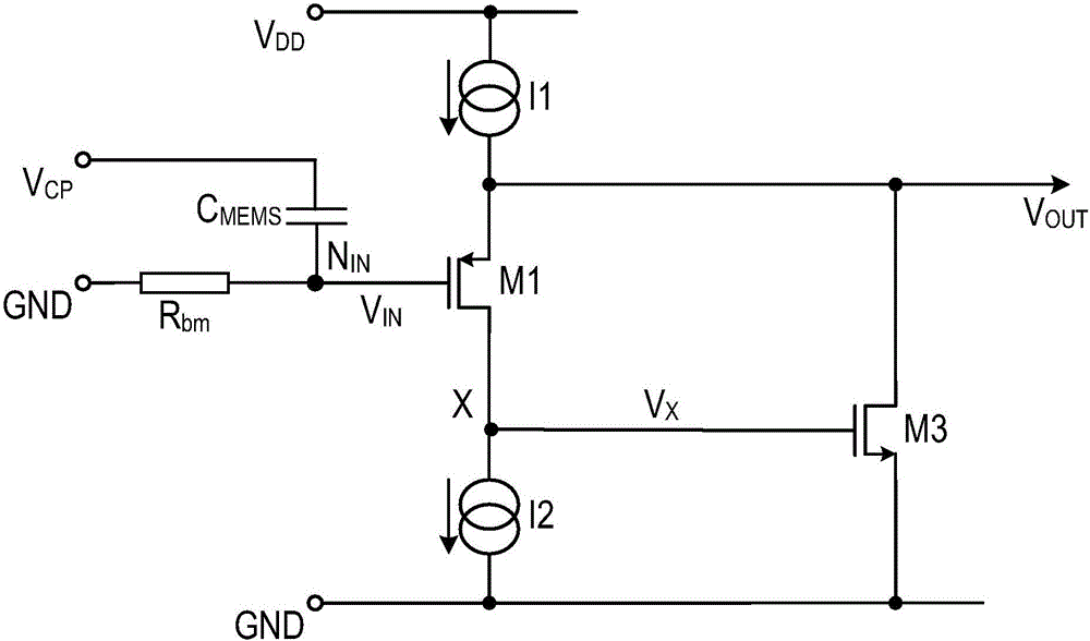
[0075] The present invention provides a preamplifier circuit that uses a super source follower to maintain low output impedance and stable signal gain.

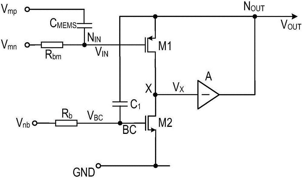
[0076] As discussed above, in some applications a relatively simple amplifier may be more suitable than a conventional long-tailed pair input stage. However, conventional source follower arrangements can suffer from load-dependent gain and distortion of large output signals. The use of a class A super source follower can provide a smaller output impedance than a conventional source follower, while requiring a smaller supply current. figure 2 An amplifier is shown that includes a super source follower arrangement. This implementation of the MEMS transducer amplifier includes a Class A super source follower. There are two MOS transistors M1 and M3, in this embodiment M1 is a PMOS transistor and M3 is an NMOS transistor. There are also constant current sources I1 and I2 connected as shown. These can also be implemented usin...


PUM


Abstract

This application relates to amplifier circuitry for amplifying a signal from a MEMS transducer. A super source follower circuit (40) is provided which includes a feedback path from its output node (Nout) to a control bias node (BC) in order to provide a preamplifier signal gain that may be greater than unity. A first transistor (M1) is configured to have its gate node connected to an input node (NIN) for receiving the input signal (VIN) and its drain node connected to an input node (X) of an output stage (A). The source node of the first transistor is connected to the output node (NOUT). A current source (I2) is configured to deliver a current to the drain node of the first transistor (M1), wherein the current source (I2) is controlled by a bias control voltage (VBC) at the bias control node (BC). A feedback impedance network (Z1) comprising a first port connected to the output node (NOUT) and a second port connected to the bias control node (BC) is provided.

Description

technical field [0001] The present invention relates to methods and apparatus for amplifying signals from MEMS capacitive transducers, and in particular to the use of super source follower based low noise preamplifiers. Background technique [0002] figure 1 A MEMS microphone 2, an associated amplifier 4 and bias circuitry 6 are shown. boosted by charge pump 8 from the supply voltage V DD derived regulated voltage V R , to utilize an appropriate voltage V CP , such as 12V, to bias the capacitive transducer 2 (C MEMS ) of a terminal. The other terminal of the capacitive transducer 2 is biased via a very high impedance 10 (for example of the order of 10 GΩ) to another fixed voltage, usually ground. One example of the type of component that can be used to create this impedance is a polysilicon diode network. Acoustic waves incident on the capacitive transducer 2 will cause one electrode plate to displace, thus changing its separation from the other electrode plate, thus ...

Claims


Application Information

Patent Timeline
Patent Type & Authority Applications(China)
IPC IPC(8): H03F1/26H03F1/34H03F3/45
CPCH03F1/0205H03F3/187H03F3/505H03F2200/15H03F2200/24H03F2200/294H03G1/0088H04R3/00H04R19/005H04R19/04H03F1/38H03G1/0094H03F1/26H03F3/183H03F2200/03H03F2200/129H04R2201/003
Inventor S·艾斯特吉曼斯
Owner CIRRUS LOGIC INT SEMICON
Why Eureka
Try Eureka