Packaging structure and packaging method of micro-electromechanical system (MEMS) sensor

A packaging structure and sensor technology, which is applied to the coupling of electric solid devices, semiconductor devices, and optical waveguides, can solve problems such as large differences in thermal expansion coefficients, MEMS chip deformation of MEMS sensor chips, and failure of MEMS sensor chip devices. Small-impact, overall performance-improving effect

Active Publication Date: 2015-11-11
INST OF GEOLOGY & GEOPHYSICS CHINESE ACAD OF SCI
View PDF3 Cites 13 Cited by
  • Summary
  • Abstract
  • Description
  • Claims
  • Application Information

AI Technical Summary

Problems solved by technology

Most of the current mainstream MEMS sensor chips are made of silicon materials, while the ceramics used in traditional ceramic packaging methods are mostly alumina and aluminum nitride. The thermal expansion coefficient of this material and the material (silicon) of MEMS sensor chips is quite different. , when the temperature of the packaged or packaged device changes, different materials shrink or expand in different degrees, and the resulting stress mismatch will cause deformation of the package shell of the MEMS sensor chip and the MEMS chip itself, thereby affecting the MEMS sensor chip. The performance of the sensor chip device, or even directly lead to the failure of the MEMS sensor chip device

Method used


Image

  • Packaging structure and packaging method of micro-electromechanical system (MEMS) sensor
  • Packaging structure and packaging method of micro-electromechanical system (MEMS) sensor
  • Packaging structure and packaging method of micro-electromechanical system (MEMS) sensor

Examples


Embodiment Construction

[0052] The technical solution of the present application will be described in further detail below in conjunction with the accompanying drawings.

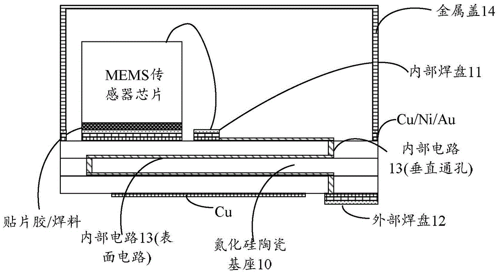
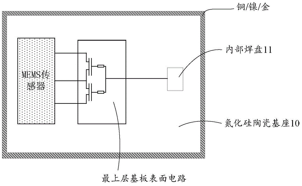
[0053] figure 1 is a cross-sectional view of a package structure of a MEMS sensor according to an embodiment of the present application, figure 2 It is a schematic top view of the package structure of the MEMS sensor according to an embodiment of the present application after the metal cover is removed. The packaging structure of the MEMS sensor of the embodiment of the present application is used to package the MEMS sensor chip made of silicon material. The packaging structure includes: a silicon nitride ceramic base 10, an internal pad 11, an external pad 12, an internal circuit 13, a metal Cover 14.

[0054] Wherein, the silicon nitride ceramic base 10 is used to fix the MEMS sensor chip, preferably fixed at the center position of the silicon nitride ceramic base 10; the silicon nitride ceramic base 10 may include at least on...


PUM

PropertyMeasurementUnit
thicknessaaaaaaaaaa
thicknessaaaaaaaaaa
thicknessaaaaaaaaaa

Abstract

The invention provides a packaging structure and a packaging method of a micro-electromechanical system (MEMS) sensor. The packaging structure comprises a silicon nitride ceramic base, an internal bonding pad, an external bonding pad, an internal circuit and a metal cover, wherein the silicon nitride ceramic base is used for fixing an MEMS sensor chip; the internal bonding pad is located on the upper surface of the silicon nitride ceramic base and is connected with a signal output end of the MEMS sensor chip; the external bonding pad is located on the lower surface of the silicon nitride ceramic base; the internal circuit is connected with the internal bonding pad and the external bonding pad; and the metal cover is fixed on the upper surface of the silicon nitride ceramic base. According to the packaging structure and the packaging method, the effects on the device performance of the MEMS sensor due to package thermal stress are effectively reduced, so as to improve the whole performance of the sensor.

Description

technical field [0001] The present application relates to the technical field of component packaging, and in particular to a packaging structure and packaging method of a MEMS (Micro-Electro-Mechanical System, Micro-Electro-Mechanical System) sensor. Background technique [0002] MEMS (micro-mechanical system) is an emerging technology developed on the basis of traditional integrated circuit technology. It realizes sensing or executive functions by fabricating micron-scale mechanical structures. Due to the large difference between its size and the conventional functional modules of millimeters or centimeters, it is necessary to realize the mutual transmission of electrical signals between modules of different scales through packaging. It is possible to reduce the impact on the MEMS chip, and at the same time protect the MEMS chip from the influence of external environmental disturbance factors. [0003] The packaging of traditional MEMS sensor chips mainly includes three me...

Claims


Application Information

Patent Timeline
Patent Type & Authority Applications(China)
IPC IPC(8): H01L23/043H01L23/31B81B7/02
CPCH01L2224/32225H01L2224/48091H01L2224/48227H01L2224/73265H01L2924/00014H01L2924/00
Inventor 郭士超
Owner INST OF GEOLOGY & GEOPHYSICS CHINESE ACAD OF SCI
Why Eureka
Try Eureka