Silicon carbide trench gate power metal-oxide-semiconductor field effect transistors (MOSFETs) device and manufacturing method thereof

A silicon carbide trench and silicon carbide technology, which is applied in semiconductor/solid-state device manufacturing, semiconductor devices, electrical components, etc., can solve the problem of unacceptable device threshold voltage and on-resistance, low effective electron mobility on the surface of the inversion layer, and electronic Effects of effective mobility and other issues, to achieve the effect of improving effective mobility, improving anti-latch-up ability, and avoiding high threshold voltage

Inactive Publication Date: 2015-11-11
GLOBAL ENERGY INTERCONNECTION RES INST CO LTD +2
View PDF3 Cites 17 Cited by
  • Summary
  • Abstract
  • Description
  • Claims
  • Application Information

AI Technical Summary

Problems solved by technology

The problem with this structure is that it is difficult for the p-base region to form an effective inversion layer channel on the surface adjacent to the gate dielectric layer, and the effective electron mobility on the surface of the inversion layer is low, which will cause the threshold voltage and on-resistance of the device to reach unacceptable level
This ion implantation process will negatively affect the effective mobility of electrons in the channel surface accumulation layer

Method used


Image

  • Silicon carbide trench gate power metal-oxide-semiconductor field effect transistors (MOSFETs) device and manufacturing method thereof
  • Silicon carbide trench gate power metal-oxide-semiconductor field effect transistors (MOSFETs) device and manufacturing method thereof
  • Silicon carbide trench gate power metal-oxide-semiconductor field effect transistors (MOSFETs) device and manufacturing method thereof

Examples


Embodiment 1

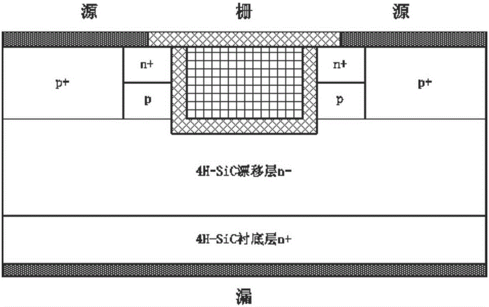
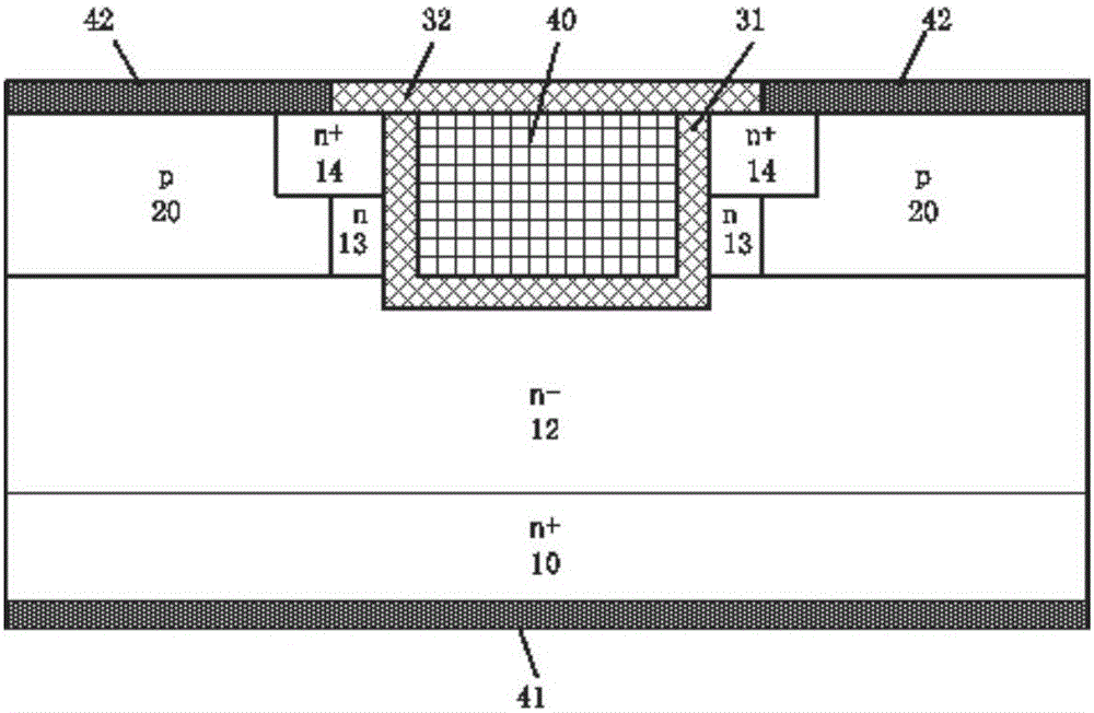
[0081] The device fabrication of the embodiment of the present invention can refer to Figure 4-12 description, as in Figure 4 On the n-type silicon carbide substrate 10 shown and the n-type silicon carbide drift layer 12 thereon, an ion implantation mask is formed and patterned, and p-type doped impurity aluminum is implanted into the n-type layer 12 to form a Figure 5 P-wells 20 are shown with a certain spacing.

[0082] Such as Figure 6 As shown, an n+ silicon carbide source region 14 is formed on the p well 20 and the n-type silicon carbide drift layer 12 by fabricating a masking film and patterning it and implanting nitrogen ions.

[0083] Such as Figure 7 As shown, continue to implant low dose nitrogen doped impurities to provide an n-type doped region for forming an n-type channel 13 between the p-type silicon carbide regions 20 .

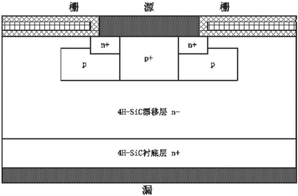
[0084] Such as Figure 8 As shown, a masking film is formed and patterned in the region corresponding to the n+ silicon carbide so...


PUM

PropertyMeasurementUnit
thicknessaaaaaaaaaa

Abstract

The invention provides a silicon carbide trench gate power metal-oxide-semiconductor field effect transistors (MOSFETs) device and a manufacturing method thereof. The device comprises an n-type silicon carbide substrate, an n-type trench, a trench gate medium, a gate contact, a source contact and a drain contact, wherein an n-type silicon carbide drift layer is arranged on the substrate, and comprises p-type silicon carbide regions with intervals; an n+ silicon carbide source region is formed between the p-type silicon carbide regions; and the n-type trench is located between the p-type silicon carbide regions and is arranged in the n-type silicon carbide drift layer below the n+ silicon carbide source region. On the basis of a vertical double-injection MOSFET structure, the surface of the trench is counter-doped with an n-type doped impurity, so that a surface accumulation layer is realized; reduction of the effective electron mobility of the surface accumulation layer of the trench caused by high-energy and large-dose ion injection and high-temperature annealing is avoided; performance degradation of the device is reduced; the anti-latch-up capacity is improved; the manufacturing method of the silicon carbide MOSFET device is simplified; and the silicon carbide trench gate power MOSFETs device is suitable for industrial production.

Description

technical field [0001] The invention relates to a semiconductor device and a manufacturing method thereof, in particular to a silicon carbide trench gate power MOSFETs device and a manufacturing method thereof. Background technique [0002] SiC materials have the characteristics of high critical field strength and high thermal conductivity. SiC MOSFET devices can theoretically realize a high-voltage and high-power semiconductor switch that is more ideal than the existing silicon IGBT. However, enhancement-mode vertical SiC power MOSFET devices with high current, high voltage and low on-resistance are still difficult to realize, partly because of the high doping concentration in the base region of high-voltage SiC MOSFETs, which makes it difficult to form an effective inversion conduction channel, and The effective mobility of channel carriers is low. [0003] Trench gate silicon carbide MOSFET structure as attached figure 1 shown. Nitrogen or phosphorus is usually implant...

Claims


Application Information

Patent Timeline
Patent Type & Authority Applications(China)
IPC IPC(8): H01L29/78H01L21/04
CPCH01L29/7813H01L21/0465H01L29/66068
Inventor 查祎英杨霏王方方李永平朱韫晖田亮吴昊夏经华
Owner GLOBAL ENERGY INTERCONNECTION RES INST CO LTD
Why Eureka
Try Eureka