
A kind of preparation method of parallel Gan-based LED chip

A LED chip and parallel technology, applied in the direction of electrical components, circuits, semiconductor devices, etc., can solve the problems of low production efficiency, inconsistent height, poor uniformity, etc., and achieve low cost, stable product performance, and high packaging efficiency.

Active Publication Date: 2018-06-05
SHANDONG INSPUR HUAGUANG OPTOELECTRONICS
View PDF4 Cites 0 Cited by
  • Summary
  • Abstract
  • Description
  • Claims
  • Application Information

AI Technical Summary

Problems solved by technology

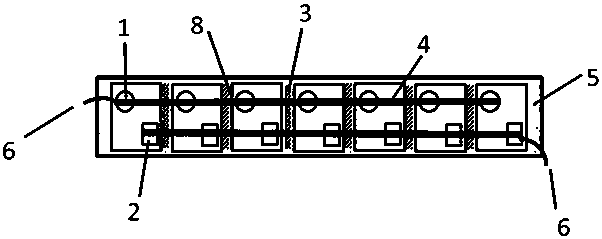
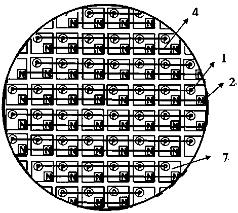
[0008] Aiming at the disadvantages of low production efficiency, poor uniformity, and inconsistent height in the packaging production and processing process of existing single LED chips, the present invention provides a parallel-connected GaN-based LED chip preparation method that is convenient for downstream customers to package, not only It can achieve high packaging efficiency, good uniformity, high stability, and can also reduce packaging costs, suitable for mass production, and greatly improve product reliability

Method used


Image

  • A kind of preparation method of parallel Gan-based LED chip
  • A kind of preparation method of parallel Gan-based LED chip

Examples


Embodiment Construction

[0032] The method for preparing parallel GaN-based LED chips of the present invention comprises the following steps:

[0033] (1) Preparation of epitaxial wafers

[0034] An epitaxial layer is grown on the sapphire substrate 5 to form an epitaxial wafer. The epitaxial layers are GaN layer, N-type GaN layer, quantum well active region and P-type GaN layer from bottom to top. In order to effectively activate the activity of doping impurities in the P-type GaN layer, a layer with a thickness of The ITO transparent conductive layer.

[0035] (2) Half-cutting the epitaxial wafer

[0036] The epitaxial wafer is cut vertically and horizontally according to the size of a single chip unit 7 with a laser scribing machine, with a cutting depth of 6-7um, to the substrate 5, so that isolation grooves 8 are formed between adjacent chip units 7.

[0037] (3) Fill the isolation groove to ensure the insulation between chip units

[0038] On the surface of the epitaxial wafer, polyimide 3...


PUM


Abstract

A method for preparing a parallel GaN-based LED chip, comprising the following steps: 1) preparing an epitaxial wafer; vapor-depositing a layer of transparent conductive layer on the surface of the epitaxial wafer; (2) cutting the epitaxial wafer to form a single chip unit, cutting to the substrate At the bottom, isolation grooves are formed between adjacent chip units; (3) Fill isolation grooves to ensure insulation between chip units; (4) Prepare N electrodes; (5) Prepare P electrode patterns, N electrode patterns and connecting electrode patterns ; (6) Evaporate metal on the P electrode pattern, N electrode pattern and connecting electrode pattern to realize chip parallel connection; (7) Deposit SiO2 protective layer on the chip surface; (8) Cut the lobes laterally to make independent parallel LED chips . The invention can realize the advantages of convenient operation in the encapsulation process, high encapsulation efficiency, low cost, stable product performance, high luminous efficiency, etc., is suitable for mass production, and can greatly improve product reliability.

Description

technical field [0001] The purpose of the present invention is to provide a method for preparing parallel GaN-based LED chips, so as to realize the connection of multi-chips during chip production, so that downstream customers only need to wire on specific electrodes when packaging, and the chip uniformity Consistent, greatly reduces the difficulty of packaging, improves the stability of the chip after packaging, and belongs to the technical field of LED chip preparation. Background technique [0002] As the core component of semiconductor lighting, LED chips are faced with increasingly severe market conditions, and higher requirements are put forward for the manufacturing methods of LED chips in terms of how to increase the optical power of chips, improve packaging efficiency, and reduce packaging costs. Traditional high-power LED chips (such as 5W, 10W, etc.) are mostly obtained by packaging the pads of multiple LED chips in parallel in a bracket with a circuit structure i...

Claims


Application Information

Patent Timeline
Patent Type & Authority Patents(China)
IPC IPC(8): H01L33/32H01L33/52H01L33/62
CPCH01L33/32H01L33/52H01L33/62
Inventor 曹志芳夏伟徐现刚闫宝华
Owner SHANDONG INSPUR HUAGUANG OPTOELECTRONICS
Learn More