Manufacturing method for printed circuit board covered with coating copper layers

A technology for printed circuit boards and manufacturing methods, applied in the directions of printed circuit manufacturing, printed circuits, manufacturing printed circuit precursors, etc., can solve problems such as difficulty, thickness of copper on circuit boards, unfavorable fine lines, etc., and increase the contact area. , the effect of strong bonding strength

Inactive Publication Date: 2015-11-11
SHENZHEN SUNTAK MULTILAYER PCB
View PDF5 Cites 6 Cited by
  • Summary
  • Abstract
  • Description
  • Claims
  • Application Information

AI Technical Summary

Problems solved by technology

This method has the following defects: the copper thickness of the circuit board after production includes bottom copper, cladding copper and covering copper, and the copper thickness of the circuit board is relatively thick, which is not conducive to the production of fine lines; and the grinding times need to be controlled during the resin grinding process and copper reduction to avoid excessive grinding
This method has the following defects: the production of the anti-alkali corrosion layer requires special equipment, which is not available in general factories, and it is difficult to apply in practice

Method used


Image

  • Manufacturing method for printed circuit board covered with coating copper layers
  • Manufacturing method for printed circuit board covered with coating copper layers
  • Manufacturing method for printed circuit board covered with coating copper layers

Examples


Embodiment

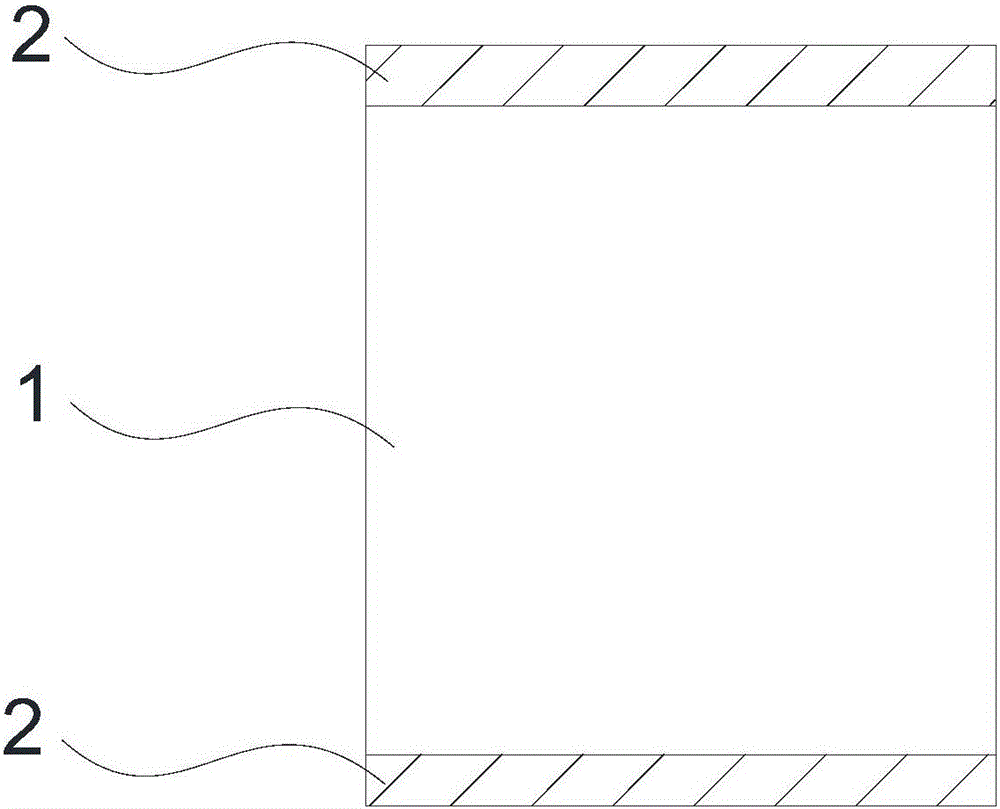
[0026] The anti-wrinkle method is used for typesetting and laminating the multi-layer board, and the following is obtained: figure 1 As shown in the circuit board, the circuit board includes a substrate 1 and copper foils 2 located on opposite surfaces of the substrate;

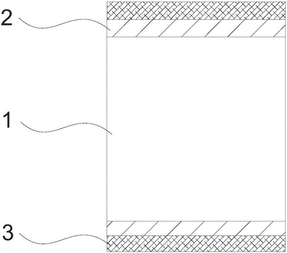
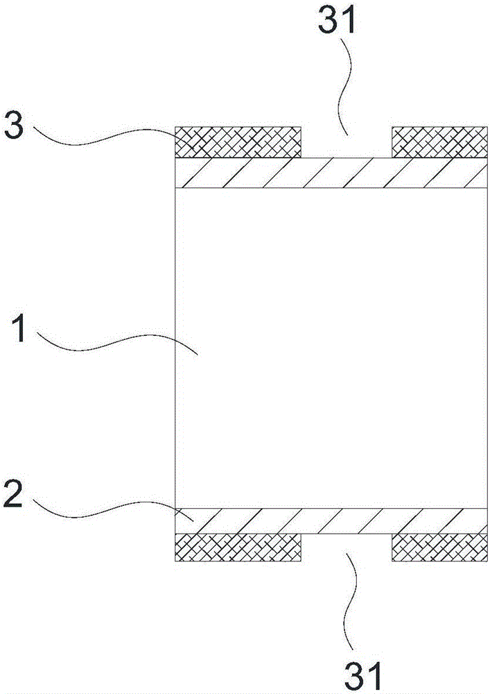
[0027] like figure 2 As shown, the circuit board is coated with dry film 3 on both sides after super-roughening treatment; image 3 As shown, after exposure and development, the dry film is made to form a circular window 31 corresponding to the position where the groove needs to be formed to expose the bottom copper. ).

[0028] Place the circuit board after the above treatment on the copper foil of a certain depth etched by the copper wire; control the Cu in the etching cylinder 2+ The concentration is 110-150g / L, the specific gravity is 1.23-1.33, the acidity is 1.5-3.8N, the temperature is 48-52°C, and the upper pressure is controlled at 0.8-2.0kg / cm 2 , the downforce is controlled at 0.8-1.5kg / cm 2 ...


PUM

PropertyMeasurementUnit
thicknessaaaaaaaaaa
depthaaaaaaaaaa
depthaaaaaaaaaa

Abstract

The invention discloses a manufacturing method for a printed circuit board coveried with coating copper layers, and relates to the circuit board production and manufacturing technology field. The manufacturing method comprises the following steps: firstly, a circuit board with a surface covered with copper foil is provided, part of copper is etched in a position, corresponding to a position of the circuit board needing drilling of a through hole, of the copper foil surface, thus a recess groove is formed in the copper foil surface, and the size of the recess groove is more than the hole diameter of through hole; secondly, the through hole in the first step is drilled; thirdly, full plate electroplating is carried out, and thus the surface of the circuit board and the inner wall of the through hole are covered with copper layersl fourthly, the through hole is subjected to resin filling, the resin for filling is subjected to flatting processing, and thus the outer surface of the covering copper layer is flat. The manufacturing method facilitates to remove the filling resin at the dense hole, manufacturing of copper coating is carried out after part of the recess groove is subjected to electrocoppering, and electrocoppering in the recess groove leaves copper reduction allowance for board wearing, and facilities flatting processing of the hole position. In addition, the contact area of the covered copper layer and the surface copper foil of the circuit board are increased, and the bonding strength is high.

Description

technical field [0001] The invention relates to the technical field of circuit board production, in particular to a method for manufacturing a printed circuit board with a copper-clad layer. Background technique [0002] At present, the production method of a printed circuit board with a copper clad layer is as follows: after the ordinary copper clad board is drilled through the hole, the board electrician will plate the copper thickness of the hole copper and the surface copper to a certain thickness, fill the hole with resin, and wait for the resin to cure. , Grinding excess resin, controlling the number of grinding times and the amount of copper reduction, and completing the copper clad production. This method has the following defects: the copper thickness of the circuit board after production includes bottom copper, cladding copper and covering copper, and the copper thickness of the circuit board is relatively thick, which is not conducive to the production of fine lin...

Claims


Application Information

Patent Timeline
Patent Type & Authority Applications(China)
IPC IPC(8): H05K3/02
CPCH05K3/022H05K2203/0789
Inventor 苗国厚曾璇刘克敢张军杰
Owner SHENZHEN SUNTAK MULTILAYER PCB
Why Eureka
Try Eureka