

Ferromagnetic semiconductor material Li (Cd, Mn) P and preparation method thereof
A semiconductor and ferromagnetic technology, applied in the direction of inorganic material magnetism, phosphide, etc., can solve the problems of physical damage, failure to obtain PN junction, difficulty in changing carrier types, etc., and achieve good semiconducting and easy to adjust effects
- Summary
- Abstract
- Description
- Claims
- Application Information
AI Technical Summary
Problems solved by technology
Method used
Image

Examples
Embodiment 1
[0044] This embodiment provides a method for preparing a ferromagnetic semiconductor material, including:
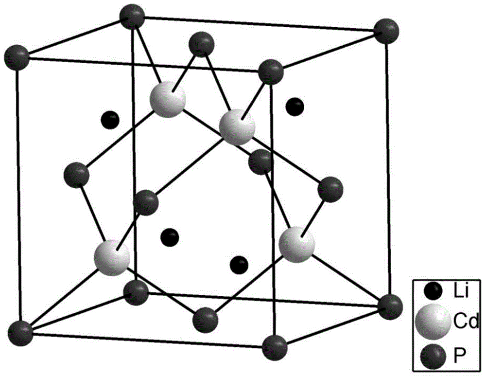
[0045] 1) In a glove box filled with inert gas, high-purity Li blocks, Cd powder, Mn powder, and P powder were mixed according to a predetermined ratio (Li 0.6 Cd 0.9 mn 0.1 P, the quality is respectively Li block 0.21 gram, Cd powder 5.06 gram, Mn powder 0.27 gram, P powder 1.55 gram) evenly mixes, and the mixture is packed in alumina ceramic test tube;
[0046] 2) Vacuum-encapsulate the ceramic test tube with the sample in the quartz tube;
[0047] 3) Put the quartz tube in a high-temperature furnace for sintering at 600°C for 20 hours, and obtain Li 0.6 Cd 0.9 mn 0.1 p.
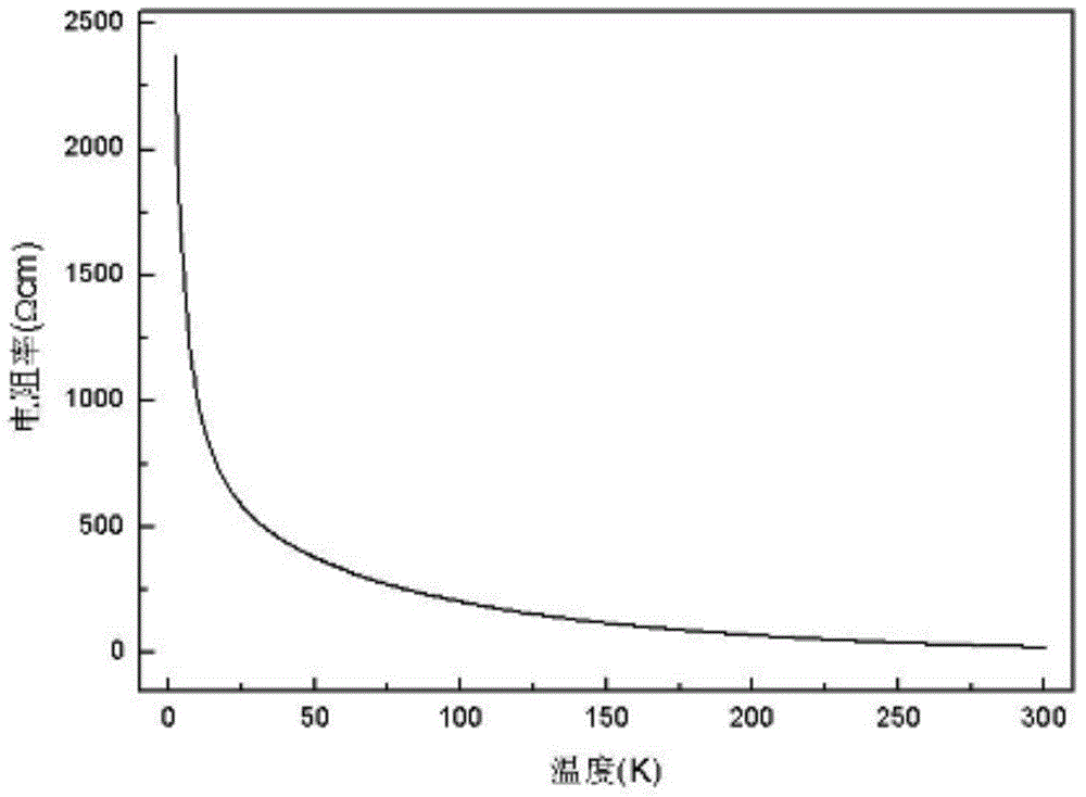
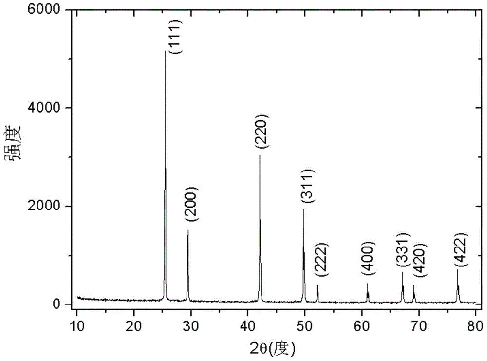
[0048] The resistivity of the sample obtained by the method of this embodiment varies with temperature behavior as figure 2 As shown, it exhibits good semiconducting properties. The X-ray diffraction pattern of the sample is as image 3 As shown, all the diffraction peaks can find the corre...
Embodiment 2
[0050] This embodiment provides a method for preparing a ferromagnetic semiconductor material, including:
[0051] 1) In a glove box filled with inert gas, high-purity Li blocks, Cd powder, Mn powder, and P powder were mixed according to a predetermined ratio (Li 1.4 Cd 0.6 mn 0.4 P, the quality is respectively 0.49 grams of Li block, 3.37 grams of Cd powder, 1.10 grams of Mn powder, 1.55 grams of P powder) uniformly mixed, and the mixture is packed in alumina ceramic test tube;
[0052] 2) Vacuum seal the ceramic test tube with the sample in the quartz tube, and fill a certain amount of inert gas into the quartz tube;
[0053] 3) Put the quartz tube in a high-temperature furnace for sintering at a temperature of 900°C for 5 hours, and obtain Li 1.4 Cd 0.6 mn 0.4 p.
[0054] The resistivity of the sample obtained by the method of this embodiment varies with temperature behavior as Figure 5 As shown, it exhibits good semiconducting properties. The X-ray diffraction pat...
Embodiment 3
[0056] This embodiment provides a method for preparing a ferromagnetic semiconductor material, including:
[0057] 1) In a glove box filled with an inert gas, the high-purity Li 3 P, P, Cd, Mn, CdP, MnP according to the predetermined ratio (Li 1.2 Cd 0.95 mn 0.05 P, with mass Li respectively 3 P1.24 gram, P0.20 gram, Cd3.37 gram, Mn0.20 gram, CdP3.87 gram, MnP0.21 gram) mix evenly, put the mixture into the niobium tube, and put the niobium tube under the protection of inert gas seal;
[0058] 2) Vacuum-encapsulate the niobium tube in the quartz tube;
[0059] 3) Put the quartz tube in a high-temperature furnace and sinter it at 750°C for 15 hours. After the sintering is completed, Li 1.2 Cd 0.95 mn 0.05 p.
[0060] The resistivity of the sample obtained by the method of this embodiment varies with temperature behavior as Figure 8 As shown, it exhibits good semiconducting properties. The X-ray diffraction pattern of the sample is as Figure 9 As shown, the correspo...
PUM
| Property | Measurement | Unit |
|---|---|---|
| Ferromagnetic transition temperature | aaaaa | aaaaa |
| Ferromagnetic transition temperature | aaaaa | aaaaa |
| Ferromagnetic transition temperature | aaaaa | aaaaa |
Abstract
Description
Claims
Application Information