Line information and non-line area information extraction method, line defect detection method

A line information, non-line technology, applied in the field of line information and non-line area information extraction, line defect detection, can solve the problem of not being able to accurately find HDI boards and IC substrates, defects, etc.

Active Publication Date: 2017-11-21
UTECHZONE CO LTD
View PDF6 Cites 0 Cited by
  • Summary
  • Abstract
  • Description
  • Claims
  • Application Information

AI Technical Summary

Problems solved by technology

[0002] In the existing printed circuit board integrated circuit manufacturing method, a conductor pattern is deposited on the printed circuit board to form it. In recent years, the development of printed circuit board technology has made the effective circuit layout space reach the limit. Density planning (the number of devices per square centimeter gradually increases), thin line and space planning of circuit board layout, increasing pitch density grid array devices, etc. Therefore, the conductor pattern formed on the printed circuit board must be relatively miniaturized and the best layout should be planned Density, so it is easy to cause defects in the circuit on the printed circuit board, so it is often necessary to further inspect and test the circuit, but with the continuous improvement of production technology, the density and diversity of printed circuit boards are rapidly increasing. Defects on HDI boards and IC substrates cannot be accurately found by visual inspection. Therefore, automated machine vision inspection methods, such as Automated Optical Inspection (AOI) or Automatic Image Inspection (AVI), are used to detect defects. Line defects on printed circuit boards are quite common

Method used


Image

  • Line information and non-line area information extraction method, line defect detection method
  • Line information and non-line area information extraction method, line defect detection method
  • Line information and non-line area information extraction method, line defect detection method

Examples


Embodiment Construction

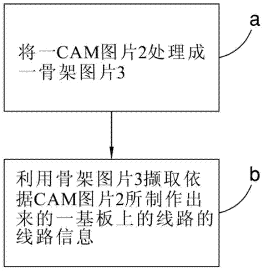
[0054] Figure 1A A flowchart showing a first preferred embodiment of a method for extracting line information of the present invention, which includes the following steps a~b:

[0055] a) Process a computer-aided design picture (hereinafter referred to as CAM picture 2 ) into a skeleton picture 3 .

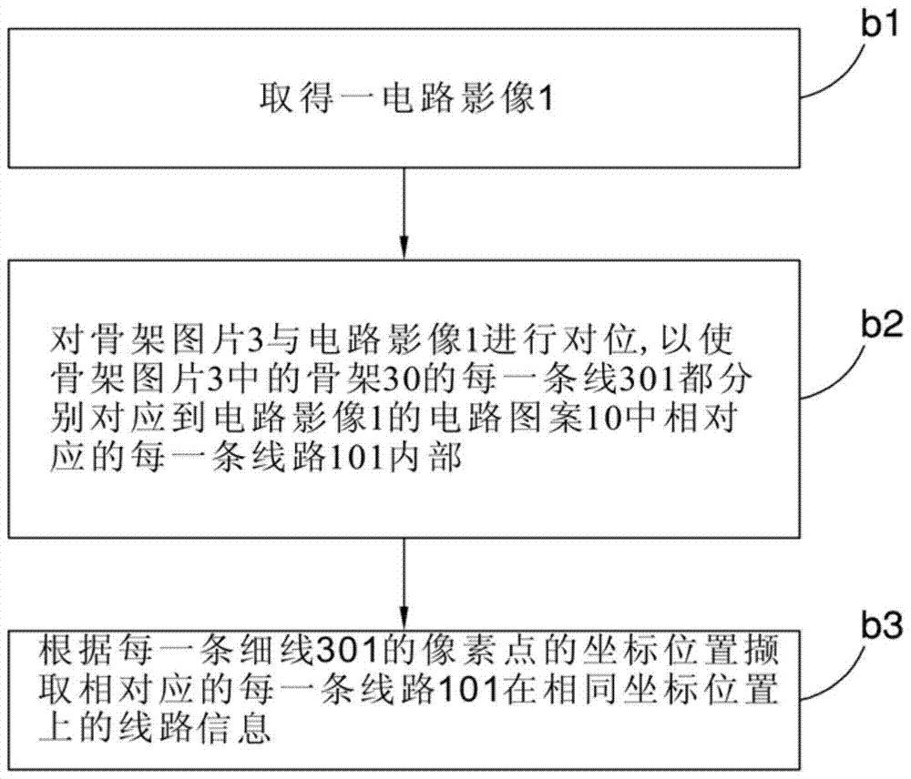
[0056] b) Use the skeleton picture 3 to extract the line information of each line or specified line on a substrate (such as a printed circuit board) produced according to the CAM picture 2, such as the color scale or line width of each line or specified line and other information. The circuit referred to here generally refers to the conductors formed on the substrate, not limited to the form of wires, for example, conductors in the form of metal pads, solder balls, metal rings, metal pins, etc. belong to it.

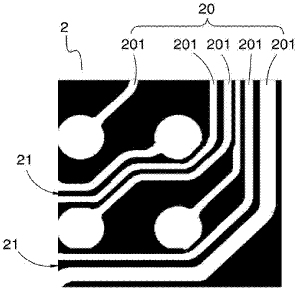
[0057] The CAM picture 2 illustrated in step a is as figure 2 As shown, it includes a CAM circuit pattern 20 (the white part in the figure) and a non-CAM circuit pattern...


PUM


Abstract

The present invention mainly discloses a method for extracting line information and non-line area information, and a line defect detection method. The line information extraction method includes processing a computer-aided design image into a skeleton image, and the skeleton image is composed of a plurality of thin lines. The skeleton, each thin line is the thinning result of each line corresponding to the computer-aided design picture; obtain the circuit image, the circuit image is taken from the substrate made according to the computer-aided design picture; the skeleton picture Align with the circuit image, so that each thin line of the skeleton in the skeleton picture corresponds to the interior of each corresponding line in the circuit image; and according to the pixel points of each thin line of the skeleton The coordinate position of each line on the circuit image corresponding to the line information at the same coordinate position is retrieved. The invention can use the obtained circuit information to detect circuit defects to find out the defects existing on the substrate.

Description

technical field [0001] The present invention relates to a method for detecting or measuring circuits on substrates such as printed circuit boards and TFT panels, especially a method for extracting circuit images captured from the substrate by using a skeleton, which can be applied to circuit defect detection or other Applied method. Background technique [0002] In the existing printed circuit board integrated circuit manufacturing method, a conductor pattern is deposited on the printed circuit board to form it. In recent years, the development of printed circuit board technology has made the effective circuit layout space reach the limit. Density planning (the number of devices per square centimeter gradually increases), thin line and space planning of circuit board layout, increasing pitch density grid array devices, etc. Therefore, the formation of conductor patterns on printed circuit boards must be relatively miniaturized and the best layout should be planned Density, ...

Claims


Application Information

Patent Timeline
Patent Type & Authority Patents(China)
IPC IPC(8): G01N21/956G01R31/02
Inventor 郑雅芸廖佐华陆家梁
Owner UTECHZONE CO LTD
Why Eureka
Try Eureka