Method and device for identifying distribution state of silicon wafer based on ultrasound

An identification method and technology for silicon wafers, which are applied in semiconductor/solid-state device manufacturing, semiconductor/solid-state device testing/measurement, electrical components, etc. Chip and equipment damage, improve detection accuracy, good effect

Active Publication Date: 2018-01-26
BEIJING NAURA MICROELECTRONICS EQUIP CO LTD
View PDF7 Cites 0 Cited by
  • Summary
  • Abstract
  • Description
  • Claims
  • Application Information

AI Technical Summary

Problems solved by technology

[0007] At present, the identification of the distribution state of the silicon wafers in the batch type silicon wafer heat treatment system generally adopts a simple photoelectric signal motion scanning method to identify the distribution state of the silicon wafers on the carrier 3. When the silicon wafer is in an abnormal state such as stacked wafers, inclined wafers or no wafers, it has a certain detection effect, but if the silicon wafer is in a protruding state on the carrier 3, it cannot be detected well, that is to say, by The existing technology simply obtains abnormal or normal results, but it is still easy to cause collisions during the motion scanning process, resulting in damage to the silicon wafer or equipment, and often produces false positives and false positives

Method used


Image

  • Method and device for identifying distribution state of silicon wafer based on ultrasound
  • Method and device for identifying distribution state of silicon wafer based on ultrasound
  • Method and device for identifying distribution state of silicon wafer based on ultrasound

Examples


Embodiment Construction

[0067] In order to make the content of the present invention clearer and easier to understand, the content of the present invention will be further described below in conjunction with the accompanying drawings. Of course, the present invention is not limited to this specific embodiment, and general replacements known to those skilled in the art are also covered within the protection scope of the present invention. Secondly, the present invention is described in detail by means of schematic diagrams. When describing the embodiments of the present invention in detail, for the convenience of explanation, the schematic diagrams are not partially enlarged according to the general scale, which should not be used as a limitation of the present invention.

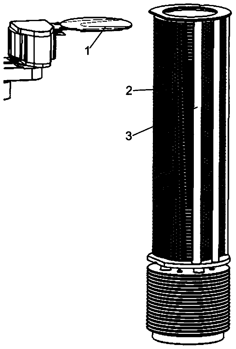
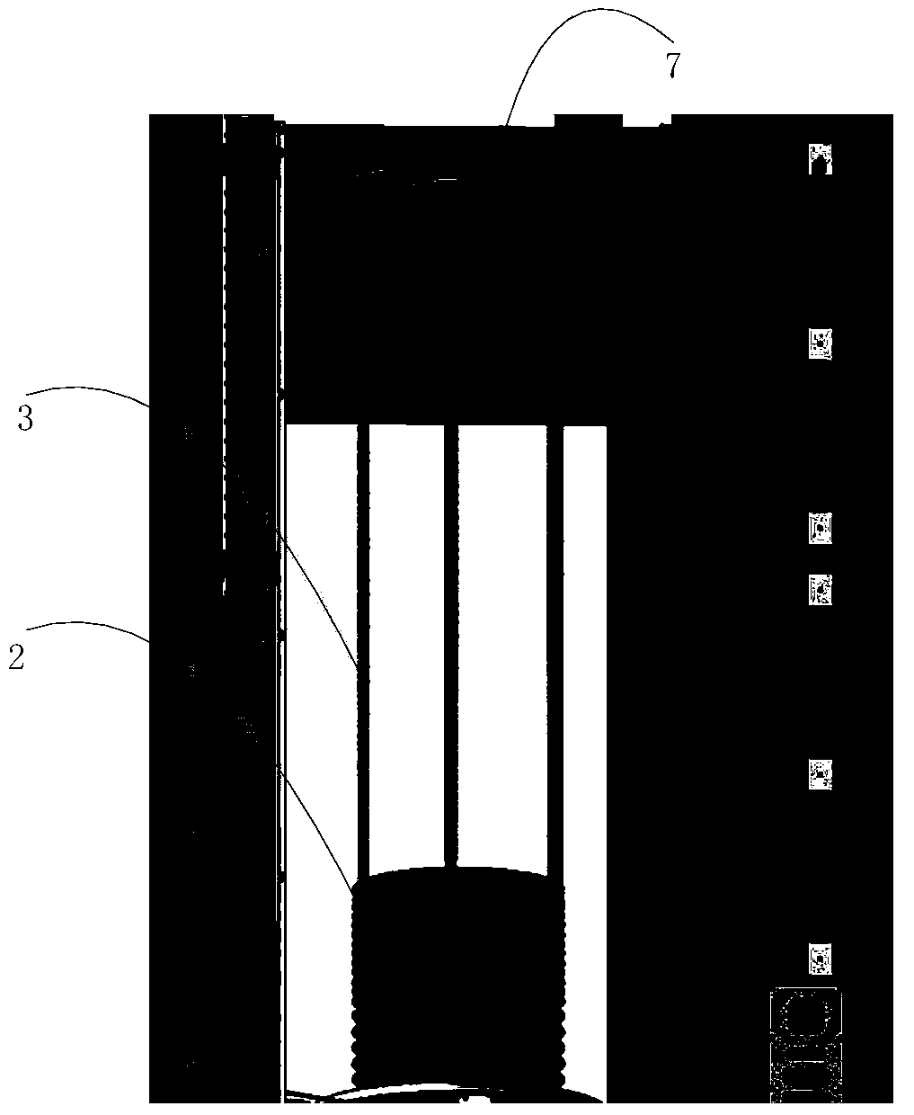
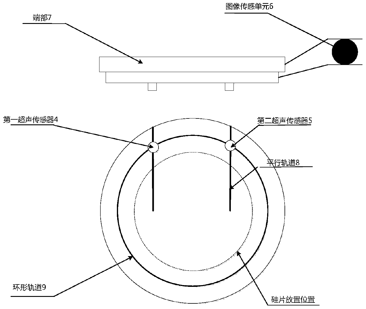
[0068] In the embodiment of the present invention, the first and second ultrasonic sensors that are symmetrical to the center of the silicon chip group are arranged in parallel above the silicon chip group, and the first and second ...


PUM


Abstract

The invention provides ultrasound-based silicon wafer distribution state recognition method and device. At two stages, namely after silicon wafers are conveyed and before the silicon wafers are taken, a first ultrasonic wave sensor and a second ultrasonic wave sensor above a silicon wafer group firstly work in a self-receiving mode, carry out an abnormal state limit position pre-scanning instruction of a protruding silicon wafer, and then carry out a silicon wafer distribution state abnormity scanning instruction through an image sensing unit on the circumferential side of a silicon wafer loader. Therefore, according to the ultrasound-based silicon wafer distribution state recognition method and device, whether abnormal distribution states of the protruding silicon wafer, an inclined silicon wafer, a laminated silicon wafer and / or a null silicon wafer exist in the region in the loader or not can be rapidly and accurately diagnosed; and a plurality of scanning detection points are distributed around the loader, so that multi-angle detection is realized; the detection accuracy is further improved; and the damages to the silicon wafers and equipment caused by manipulator movement can be well avoided. An experiment proves that the ultrasound-based silicon wafer distribution state recognition method and device are simple to realize and good in effect.

Description

technical field [0001] The present invention relates to the technical field of semiconductor processing equipment, and in particular to a method for recognizing the distribution state of silicon wafers in a bearing area of ​​semiconductor equipment based on ultrasound. The invention also relates to a device for identifying the distribution state of silicon wafers in a bearing area of ​​semiconductor equipment based on ultrasound. Background technique [0002] The safe access and transportation of silicon wafers is a very important technical indicator of large integrated circuit production lines. During the production process, it is usually required that the silicon wafer fragmentation rate caused by the transportation equipment itself should be less than one in 100,000. Moreover, as a batch silicon wafer heat treatment system, compared with a single-wafer process system, each production process requires more times of silicon wafer transmission, silicon wafer placement and rem...

Claims


Application Information

Patent Timeline
Patent Type & Authority Patents(China)
IPC IPC(8): H01L21/67H01L21/66
CPCH01L21/67294H01L22/22
Inventor 徐冬慕晓航
Owner BEIJING NAURA MICROELECTRONICS EQUIP CO LTD
Why Eureka
Try Eureka