Embedded composite meta-material absorber
A technology of metamaterials and absorbers, applied in the direction of electrical components, magnetic field/electric field shielding, etc., can solve the problems that high and low frequencies cannot be taken into account at the same time, and the thickness of low frequency absorbers is thick, so as to achieve the effect of retaining high frequency performance and strong absorption
- Summary
- Abstract
- Description
- Claims
- Application Information
AI Technical Summary
Problems solved by technology
Method used
Image
Examples
Embodiment 1
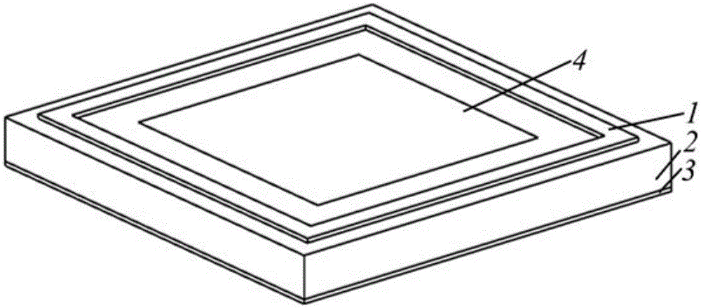
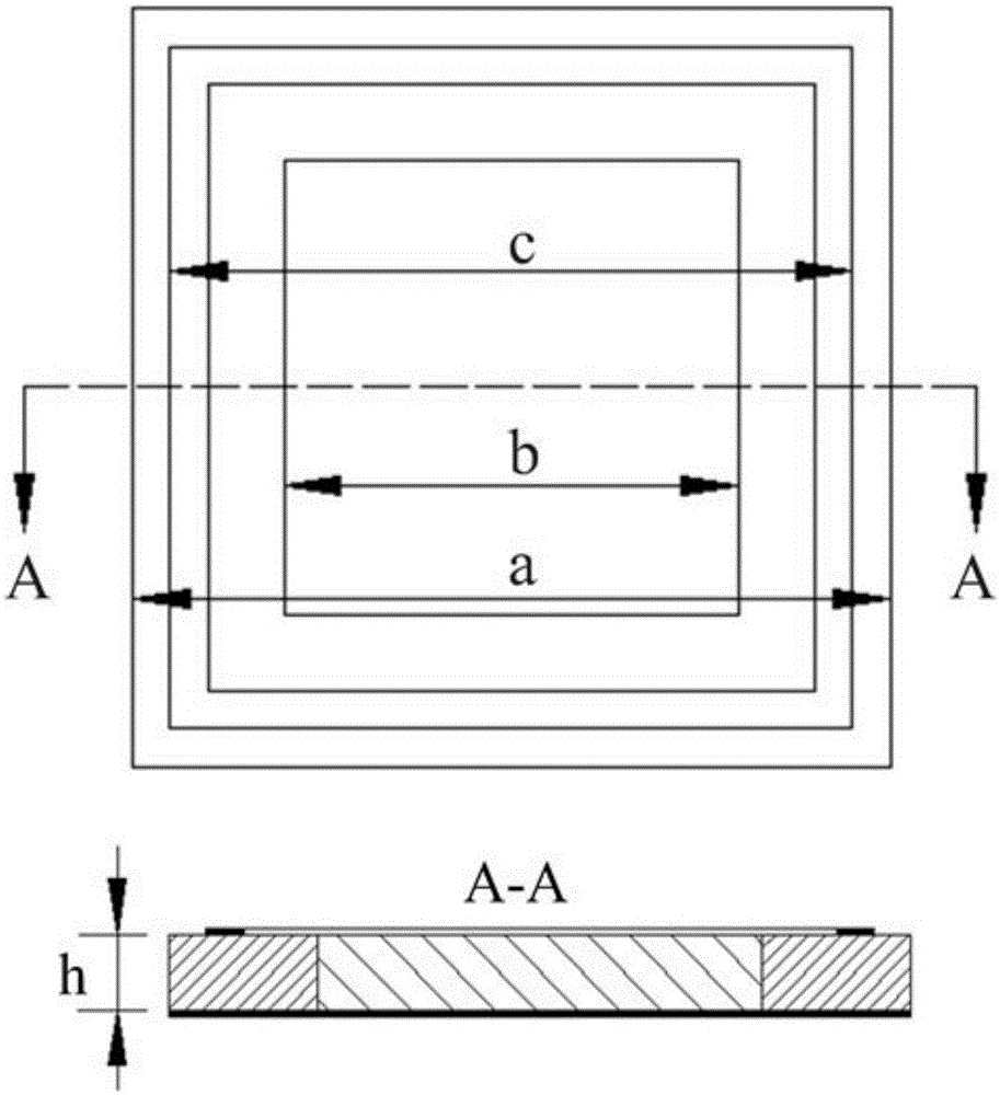
[0040] The composite metamaterial absorber unit (CMA) is embedded in a square ring, and its structure diagram is shown in figure 1 As shown, from top to bottom are: metal pattern 1 , nested structure, and metal backplane 3 , wherein the nested structure includes a patterned dielectric substrate 3 and a patterned wave-absorbing material 4 . figure 2 for figure 1 Top and cross-sectional views of the structure shown. The upper layer of the composite superstructure is a metal pattern, its material is copper, and its electrical conductivity is 5.8×10 7 s / m, the thickness is 0.017mm, the shape is a square ring, the size of the ring is 18mm, and the line width is 0.2mm. The middle layer is composed of a square ring-shaped dielectric substrate and a patterned wave-absorbing material, and the patterned wave-absorbing material is embedded in the square-ring dielectric base. figure 1 The Chinese annular dielectric matrix material is FR-4, and its dielectric parameter is ε r =4.3(1-i...
Embodiment 2
[0042] A dielectric-based superstructure (SR) with ring-shaped embedded composite metamaterial absorber units is prepared on a metal backplane, and thefigure 1 The patterned absorbing material referred to in 4 is removed to obtain the following Figure 5 Cross-sectional view of the annular dielectric-based superstructure shown. The upper layer is a circular metal pattern, its external dimension is a=18mm, and the line width of the metal ring is 0.2mm; the middle layer is, the size of the square annular dielectric substrate is: a=18.2mm, b=15.6mm, and its dielectric parameter is ε r =4.3(1-i0.025); the bottom layer is a metal backplane. Both the metal backplane and the metal pattern material are copper, and its conductivity is 5.8×10 7 s / m, the thickness is 0.017mm. The square-ring dielectric-based superstructure was prepared by circuit printed board engraving technology, and its fitting and measured absorption properties are as follows: Figure 6 As shown, the dotted line i...
Embodiment 3
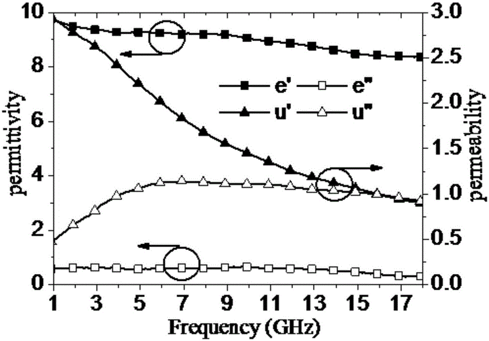
[0044] A patterned absorber (MP) with a circular embedded composite metamaterial absorber unit prepared on a metal backplane, the top view and cross-sectional view of the unit structure are shown in Figure 7 shown. It consists of a metal backplane and a block of absorbing material located above the metal backplane. The material of the metal backplane is copper, and its conductivity is 5.8×10 7 s / m, the thickness is 0.017mm, the back plate is square, and the side length is a=18.2mm; the size of the absorbing material block is b=15.6mm, the absorbing material thickness is 2mm, and the absorbing material block is surrounded by air. Firstly, the patterned wave-absorbing material is calculated by the equivalent medium theory, satisfying that the thickness is 2 mm, and the electromagnetic wave absorption rate is above 80% at 8-18 GHz. The electromagnetic parameter dispersion of the magnetic wave-absorbing material is calculated as follows: image 3 As shown, the dielectric real pa...
PUM
| Property | Measurement | Unit |
|---|---|---|
| thickness | aaaaa | aaaaa |
| thickness | aaaaa | aaaaa |
| thickness | aaaaa | aaaaa |
Abstract
Description
Claims
Application Information


