Novel wafer level tin solder micro bump manufacturing method

A fabrication method and micro-bump technology, applied in semiconductor/solid-state device manufacturing, electrical components, electrical solid-state devices, etc., can solve problems such as excessive etching and affect the reliability of micro-bumps, avoid excessive etching, reduce Interfacial connection strength, the effect of avoiding delamination failure

Inactive Publication Date: 2015-12-09
BEIJING UNIV OF TECH
View PDF9 Cites 9 Cited by
  • Summary
  • Abstract
  • Description
  • Claims
  • Application Information

AI Technical Summary

Problems solved by technology

In the existing process, the entire wafer is immersed in the etching solution when etching the UBM layer, and the isotropic wet etching is performed with the electroplated solder micro-bump as the etching mask. One of the processes The main disadvantage is the "undercut (Undercut)" problem of the electroplated copper layer, such as figure 1 shown
This is because the density of copper and titanium formed by PVD is higher than that of electroplated copper, so the electroplated copper layer on the metal copper layer under the bump is susceptible to excessive etching, and an inward recess is formed under the barrier layer. kerf, which affects microbump reliability

Method used


Image

  • Novel wafer level tin solder micro bump manufacturing method
  • Novel wafer level tin solder micro bump manufacturing method
  • Novel wafer level tin solder micro bump manufacturing method

Examples


Embodiment Construction

[0038] In order to understand the technical content of the present invention more clearly, the following embodiments are given in detail, and the above-mentioned features and advantages of the present invention are described in detail in conjunction with the accompanying drawings. Its purpose is only to better understand the content of the present invention but not to limit the protection scope of the present invention. The semiconductor packaging structure of the embodiment of the present invention can be used in the preparation of micro-bumps. But its application is not limited to this.

[0039] see Figure 2 to Figure 10 , the manufacturing process of solder micro-bumps of the present invention is as follows:

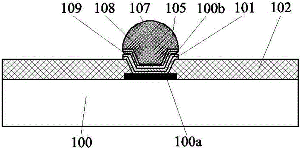
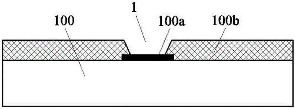
[0040] An IC wafer (100) is provided, the front side of the wafer has a passivation layer (100b) and several pads (100a), the passivation layer (100b) is formed with several first openings (1) exposing the pads ;

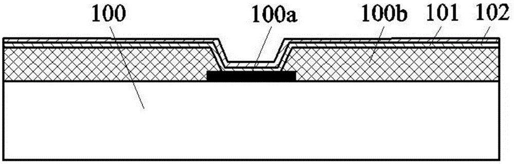
[0041] Such as image 3 As shown, an UBM titani...


PUM


Abstract

The invention provides a novel wafer level tin solder micro bump manufacturing method, and belongs to the field of semiconductor chip packaging. Photoresist of which the opening is formed through exposure development is utilized to act as a mask film firstly. A copper layer, a barrier layer and solder alloy are electroplated on an under bump metal layer in turn, and the solder alloy is enabled to completely wrap a copper layer-barrier layer of the bottom part. Then tin solder micro bumps are formed via a method of backflow and then photoresist removing. Finally the micro bumps act as an etching mask film and a wet etching technology is adopted to remove the excess under bump metal layer. Excessive etching of electroplating copper of a bump layer in isotropic etching of the under bump metal layer can be avoided, and bridging caused by collapsing of backflow of the micro bumps can be avoided so that reliability of the micro bumps and packaging products can be enhanced.

Description

technical field [0001] The invention relates to a method for manufacturing wafer-level micro-bumps, which belongs to the field of semiconductor chip packaging. Background technique [0002] With the continuous development of various electronic products in the direction of high integration, high performance, light weight and miniaturization, the packaging density of electronic packaging is also getting higher and higher, and the number of I / Os of chips is also increasing. In order to meet these requirements, advanced packaging forms such as BGA, CSP, FlipChip, etc. have been produced. But no matter what kind of packaging, wafer-level packaging is gradually becoming the mainstream packaging technology due to its advantages of high integration, reduced product cost, and shortened manufacturing time. In view of this, a key technology in wafer-level packaging - micro-bump technology is also developing in the direction of small size, fine pitch, and high density. [0003] The ex...

Claims


Application Information

Patent Timeline
Patent Type & Authority Applications(China)
IPC IPC(8): H01L21/60
CPCH01L24/11H01L24/81H01L24/94H01L2224/11
Inventor 秦飞别晓锐史戈安彤武伟肖智轶
Owner BEIJING UNIV OF TECH
Why Eureka
Try Eureka