A chip bonding method for gaas MMIC thinning process

A technology of bonding and process, applied in the direction of electrical components, semiconductor/solid-state device manufacturing, circuits, etc., can solve the problems of increasing raw materials, increasing process steps, etc., and achieve the effect of solving the problem of debris, leveling the suspension coating, and strong adhesion

Active Publication Date: 2018-06-05
GUILIN UNIV OF ELECTRONIC TECH
View PDF4 Cites 0 Cited by
  • Summary
  • Abstract
  • Description
  • Claims
  • Application Information

AI Technical Summary

Problems solved by technology

However, this method not only needs to increase the raw materials, but also needs to increase the process steps accordingly

Method used


Image

  • A chip bonding method for gaas MMIC thinning process
  • A chip bonding method for gaas MMIC thinning process
  • A chip bonding method for gaas MMIC thinning process

Examples


Embodiment 1

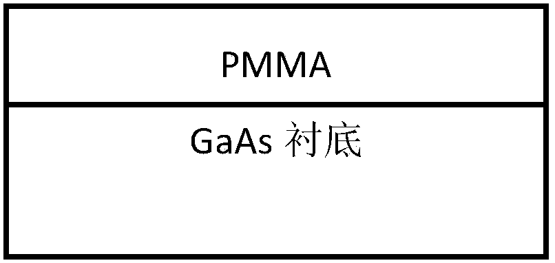
[0035] 1) Spread electron beam photoresist on the front side of GaAs substrate, such as figure 1 Shown. The electron beam photoresist is PMMA-A11 photoresist, the speed of the homogenizing table is 1500 revolutions / min, the time is 1 min, the number of leveling is 3 times, the thickness of leveling is about 5um, and the baking condition is 180℃ hot The plate is heated for 3 minutes.

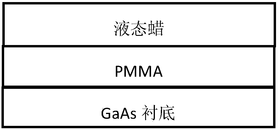
[0036] 2) Spread liquid wax evenly on the electron beam photoresist, such as figure 2 As shown; where: the liquid wax is prepared according to the following method: Weigh Crystalbond 509 strong adhesive and acetone according to the ratio of 20g:50ml, put them in the vessel, seal the vessel, and place it in a water bath at 60°C until Crystalbond 509 strong adhesive is completely dissolved and ready. When leveling liquid wax, the rotation speed of the leveling table is 1500 rpm, the time is 15sec, the number of leveling is 5, and the thickness of leveling is about 5um.

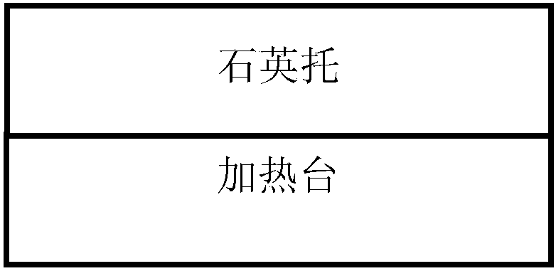
[0037] 3) Place the quartz h...

Embodiment 2

[0044] Repeat Example 1, except that the liquid wax is prepared as follows: Weigh Crystalbond 509 strong adhesive and acetone at a ratio of 10g:40ml, place them in a container, seal the container, and place it in a water bath at 50°C. Until Crystalbond 509 strong adhesive is completely dissolved, it is ready.

Embodiment 3

[0046] Repeat Example 1, except that the liquid wax is prepared as follows: Weigh Crystalbond 509 strong adhesive and acetone according to the ratio of 30g:60ml, put them in a container, seal the container, and place it in a water bath at 50°C. Until Crystalbond 509 strong adhesive is completely dissolved, it is ready.


PUM


Abstract

The invention discloses a die bonding method used for a GaAs MMIC thinning technology. The method comprises the steps of: evenly coating an electron beam photoresist on the front surface of a substrate and pasting the surface of the substrate to a quartz holder with liquid wax, wherein the liquid wax is composed of a certain amount of Crystalbond 509 strong adhesive and acetone capable of dissolving the amount of the Crystalbond 509 strong adhesive. According to the invention, the liquid wax of a special formula is used instead of conventional high-temperature wax, and in the usage environment, organic matters, which are difficult to remove and generated by mutual dissolution of the photoresist and the high-temperature wax, are prevented without adding other barrier layers; secondly, both the liquid wax and the photoresist are freely soluble in acetone, so that the problem in the conventional technology, that glue removing is slow and difficult when the high-temperature wax is used in the die bonding process, is solved; in addition, good adhesiveness is achieved between the substrate and the quartz holder, and the fragment problem in the polishing and thinning processes is effectively solved.

Description

Technical field [0001] The invention relates to a bonding method in a substrate thinning process, in particular to a bonding method used in a GaAs MMIC thinning process. Background technique [0002] In the reliability experiments of GaAs (gallium arsenide) integrated circuits, most of the samples showed that the thermal resistance of the device decreased with time over a period of time. This is due to the contact between the chip and the package due to the higher test temperature The stress has improved. For power field effect transistors (FET), thermal resistance is an important parameter. When the device is in the same power consumption and external environment, the thermal resistance is small, which can reduce the channel temperature and improve the reliability of the device in normal use. By reducing the thickness of GaAs wafers, etching through holes through GaAs wafers, and electroplating large-area metal films for heat dissipation on the back of the wafers, the thermal r...

Claims


Application Information

Patent Timeline
Patent Type & Authority Patents(China)
IPC IPC(8): H01L21/67
CPCH01L21/67092
Inventor 李海鸥曹明民林子曾周佳辉李琦韦春荣常虎东张旭芳肖功利高喜
Owner GUILIN UNIV OF ELECTRONIC TECH
Why Eureka
Try Eureka