A method for reducing the pollution of plasma etching machine cavity in GAAS back hole process

A technology of plasma etching and back hole, applied in semiconductor/solid-state device manufacturing, discharge tubes, electrical components, etc., can solve problems such as pollution, solve the problem of debris, strong adhesion, and achieve the effect of etching

Active Publication Date: 2018-07-03
GUILIN UNIV OF ELECTRONIC TECH
View PDF6 Cites 0 Cited by
  • Summary
  • Abstract
  • Description
  • Claims
  • Application Information

AI Technical Summary

Problems solved by technology

This method uses a liquid wax composed of a special formula to replace the traditional high-temperature wax. During use, there will be no miscibility problems between the liquid wax and the electron beam photoresist, and excellent adhesion between the substrate and the quartz support is ensured. At the same time, it can also effectively solve the problem of high-temperature wax and metal sputtered due to plasma bombardment contaminating the inner wall of the plasma etching machine, and improve the efficiency of the plasma etching machine

Method used


Image

  • A method for reducing the pollution of plasma etching machine cavity in GAAS back hole process
  • A method for reducing the pollution of plasma etching machine cavity in GAAS back hole process
  • A method for reducing the pollution of plasma etching machine cavity in GAAS back hole process

Examples


Embodiment 1

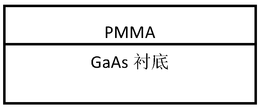
[0045] 1) Evenly coat electron beam photoresist on the front side of the GaAs substrate, such as Figure 12 shown. Among them, the electron beam photoresist is PMMA-A11 photoresist, the speed of the coating table is 1500 rpm, the time is 1min, the number of times of coating is 3 times, the thickness of the coating is about 5um, and the baking condition is 180 ℃ heat The board is heated for 3 minutes, the purpose of which is to fully volatilize the solvent in the photoresist.

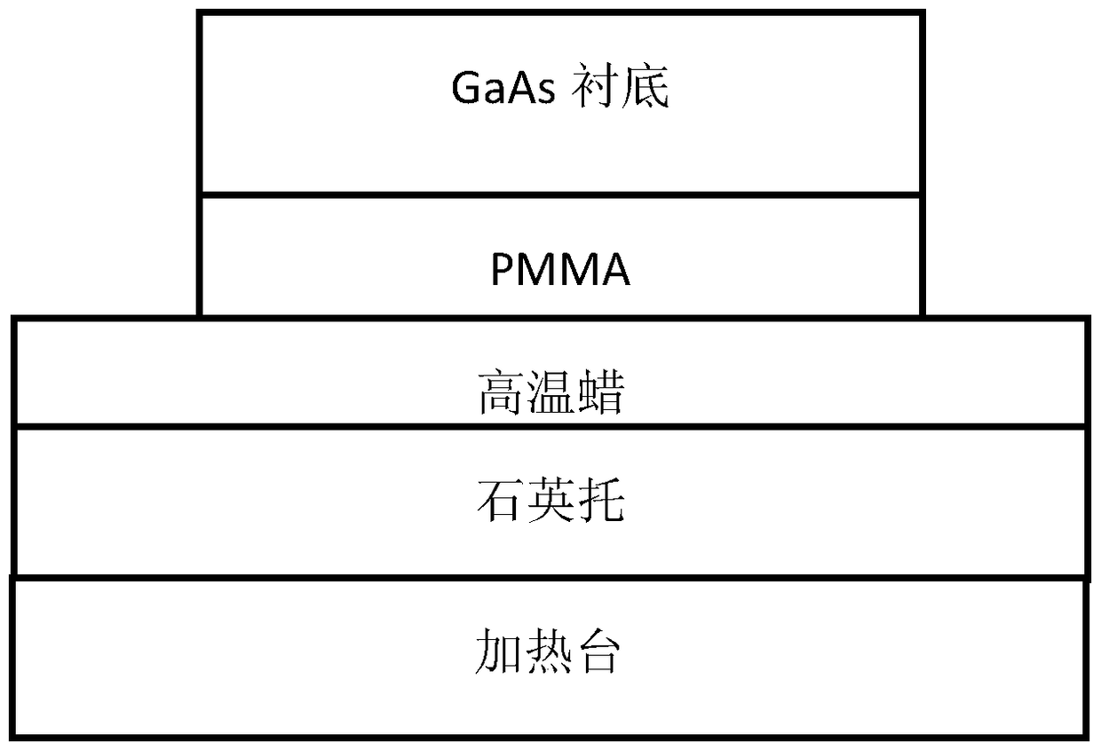
[0046] 2) Evenly coat liquid wax on the front surface of the substrate coated with electron beam photoresist, such as Figure 13 shown; wherein, the liquid wax is prepared according to the following method: Weigh Crystalbond 509 strong adhesive and acetone at a ratio of 20g: 50ml, place them in a vessel, seal the vessel, and keep it in a water bath at 60°C until Crystalbond 509 Strong Adhesive is fully dissolved and ready to use. When uniformly coating liquid wax, the speed of the coating table is 150...

Embodiment 2

[0057] Repeat Example 1, the difference is that the liquid wax is prepared as follows: Weigh Crystalbond 509 strong adhesive and acetone at a ratio of 10g: 40ml, place them in a vessel, seal the vessel, and place it in a water bath at 50°C Until the Crystalbond 509 strong adhesive is completely dissolved, that is.

Embodiment 3

[0059] Repeat Example 1, the difference is that the liquid wax is prepared as follows: Weigh Crystalbond 509 strong adhesive and acetone at a ratio of 30g: 60ml, place them in a vessel, seal the vessel, and place it in a water bath at 70°C Until the Crystalbond 509 strong adhesive is completely dissolved, that is.


PUM


Abstract

The invention discloses a method for reducing plasma etching machine cavity pollution in GaAs back hole process. The method comprises the following steps: uniformly coating an electron beam photoresist on the front face of a substrate, pasting the front face of the substrate onto a quartz tray using a liquid wax, pasting the quartz tray, to which the substrate is pasted, to a thinning glass sheet, performing thinning process, taking the quartz tray together with the substrate down from the thinning glass sheet, uniformly coating the photoresist and then baking the sheet, forming a back hole pattern, forming a back hole, and removing the photoresist and the liquid wax to enable the substrate sheet to be separated from the quartz tray; and the liquid wax is composed of a certain amount of a Crystalbond 509 strong adhesive and an amount of acetone capable of dissolving the Crystalbond 509 strong adhesive. The liquid wax is adopted to replace a traditional high-temperature wax, a mutual dissolution problem cannot be generated, the liquid wax also has excellent adhesivity, and the problems of the sputtered high-temperature wax due to plasma bombardment and metal pollution of a plasma etching machine cavity inner wall are solved.

Description

technical field [0001] The invention relates to the technical field of backhole processing of GaAs microwave devices, in particular to a method for reducing the cavity pollution of a plasma etching machine in the GaAs backhole process. Background technique [0002] As the operating frequency of GaAs microwave circuits increases, lower grounding inductance, smaller device thermal resistance, and shorter grounding distance are required. At low frequencies, bond wires are often used for grounding, and the resulting parasitic inductance is not large enough to affect circuit performance. However, when working in the microwave and millimeter wave frequency bands, this method will generate considerable grounding inductance and device thermal resistance, which will adversely affect the high-frequency characteristics of the circuit. This problem can be solved by reducing the thickness of the GaAs wafer, etching the back hole of the GaAs wafer, and electroplating a large-area metal f...

Claims


Application Information

Patent Timeline
Patent Type & Authority Patents(China)
IPC IPC(8): H01L21/3065H01J37/32
CPCH01J37/32477H01L21/3065
Inventor 李海鸥林子曾曹明民周佳辉常虎东丁志华张旭芳李琦肖功利
Owner GUILIN UNIV OF ELECTRONIC TECH
Why Eureka
Try Eureka