A nanomaterial transmission electron microscope in-situ photoelectric test chip, chip preparation method and application thereof

A photoelectric test chip, transmission electron microscope technology, applied in the direction of circuit, electrical components, final product manufacturing, etc., can solve the problem of no good solution, can not meet the nanoscale characterization of photoelectric materials, can not carry out photoelectric in situ testing and other problems, to achieve Ease of promotion, good use effect, and chip cost reduction

Active Publication Date: 2017-04-26
NANJING UNIV
View PDF3 Cites 0 Cited by
  • Summary
  • Abstract
  • Description
  • Claims
  • Application Information

AI Technical Summary

Problems solved by technology

However, the existing in-situ MEMS chip still has its limitations in application. One of the more prominent ones is that it cannot be used for photoelectric in-situ testing, which cannot meet the needs of nanoscale characterization of the actual working state and behavior of photoelectric materials.
However, this limitation limits the application of in-situ MEMS chips to a large extent, and there is currently no good solution

Method used


Image

  • A nanomaterial transmission electron microscope in-situ photoelectric test chip, chip preparation method and application thereof
  • A nanomaterial transmission electron microscope in-situ photoelectric test chip, chip preparation method and application thereof
  • A nanomaterial transmission electron microscope in-situ photoelectric test chip, chip preparation method and application thereof

Examples


Embodiment 1

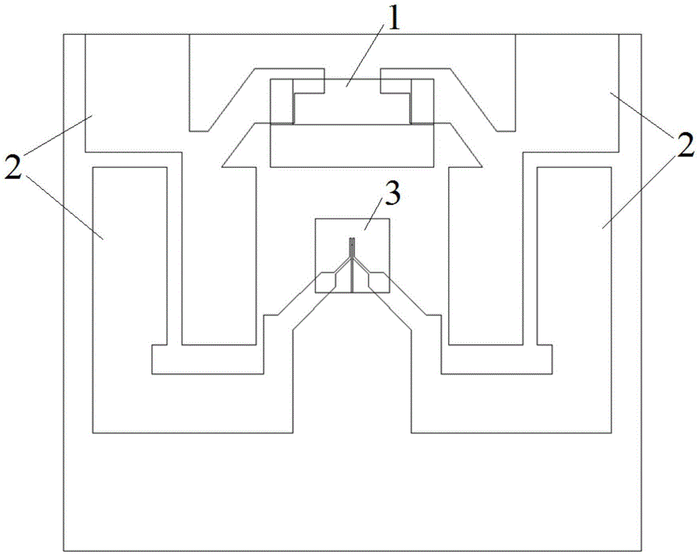
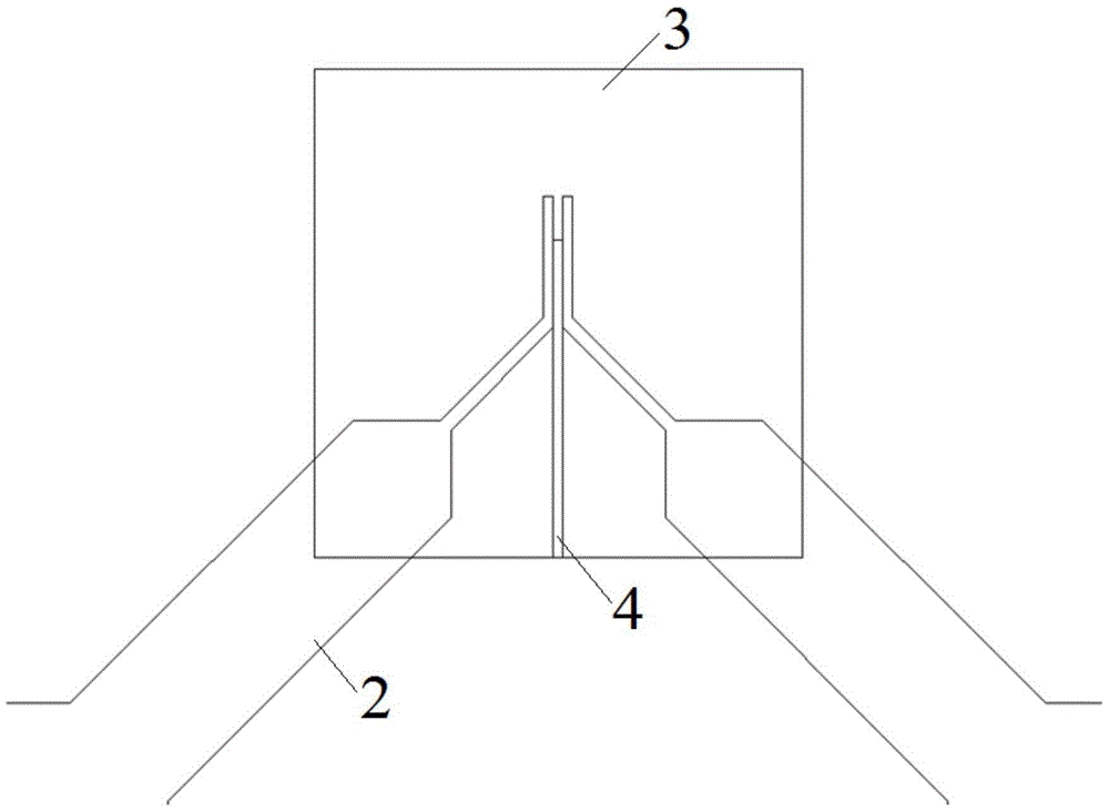
[0036] see figure 1 , figure 2 and image 3 , a nanomaterial transmission electron microscope in-situ photoelectric test chip of this embodiment, including a silicon substrate, an insulating layer, a light emitting diode (LED) 1, a metal electrode 2, a thin film window 3 and an electron beam transmission region 4. Specifically: the silicon substrate is a rectangular sheet with a thickness of 400 μm, and there are insulating layers on both sides of the silicon substrate, and the insulating layer includes a silicon dioxide layer grown on the silicon substrate and a silicon dioxide layer on the silicon dioxide layer. For the grown silicon nitride layer, the thickness of the silicon dioxide layer is 900nm, and the thickness of the silicon nitride layer is 200nm. A metal electrode 2 is formed on the front insulating layer of the silicon substrate. The thickness of the metal electrode 2 is 150nm. The metal electrode 2 is mainly used to connect with the lead wire on the sample rod...

Embodiment 2

[0060] A nanomaterial transmission electron microscope in-situ photoelectric test chip and its preparation method in this embodiment are basically the same as in Embodiment 1, except that the thickness of the silicon substrate in this embodiment is 100 μm, and the metal electrodes are located on the film window. Parts are distributed along one side of the electron beam penetrating slot, the length of the electron beam penetrating slot is 300 μm, and the width is 10 μm. The thickness of the metal electrode is 50nm, the thickness of the silicon dioxide layer in the insulating layer is 200nm, and the thickness of the silicon nitride layer is 5nm.

[0061] In this embodiment, the process of using the in-situ photoelectric test chip to transfer the nanowire sample using a micromanipulator in the laboratory is as follows:

[0062] (1) Under an optical microscope, a nanowire sample with a length of about 20 μm was picked up with the tip of a micromanipulator. Since the micromanipula...

Embodiment 3

[0069] A nanomaterial transmission electron microscope in-situ photoelectric test chip, chip preparation method and application thereof in this embodiment are basically the same as in Embodiment 1, except that the thickness of the silicon substrate in this embodiment is 200 μm, and the metal electrodes are located on the thin film. The parts on the window are distributed along both sides of a row of electron beam holes, the electron beam holes are arranged in a straight line, the distance between adjacent electron beam holes is 10 μm, the total number is 4, and the diameter of each electron beam hole is 20 μm . The thickness of the metal electrode is 200nm, the insulating layer is a silicon nitride layer, and the thickness of the silicon nitride layer is 150nm.


PUM


Abstract

The invention discloses a nanomaterial in-situ photoelectric test chip of a transmission electron microscope, a chip fabrication method and application of the chip, belonging to the technical field of in-situ test of the performance of a nanomaterial. The chip comprises a silicon substrate, insulation layers, metal electrodes, a thin-film window and a light emitting diode, wherein the insulation layers are grown on the two surfaces of the silicon substrate; the metal electrodes are grown on the insulation layer on the front surface of the chip and can be electrically connected with a sample; and the thin-film window is arranged at the center of the chip, an electron beam transmission groove or an electron beam transmission hole is formed in a region of the thin-film window, and the light emitting diode is welded on the pair of metal electrodes in front of the thin-film window. By the chip, controllable illumination can be simultaneously carried out on the samples, an electrical effect can be applied or electrical signals of the samples are received, and thus, photoelectric in-situ measurement on the transmission electron microscope sample under the atomic resolution can be achieved.

Description

technical field [0001] The invention relates to the technical field of in-situ testing of nanomaterial properties, and more specifically relates to a nanomaterial transmission electron microscope in-situ photoelectric test chip, a chip preparation method and an application thereof. Background technique [0002] Optoelectronic materials are currently one of the most concerned functional materials, and their applications involve new energy, lighting, communications, environmental protection, medical care and other aspects. Transmission Electron Microscope (TEM) is a powerful modern material characterization method, which is used to analyze the fine structure smaller than 0.2um that cannot be seen clearly under the optical microscope. Today's TEM is capable of sub-Angstrom resolution and is a powerful tool for analyzing nanomaterials. Nanomaterials have peculiar effects in the fields of electricity, heat, mechanics, etc. With the development of Micro Electromechanical System (...

Claims


Application Information

Patent Timeline
Patent Type & Authority Patents(China)
IPC IPC(8): H01L31/0216H01L31/0224H01L31/18
CPCH01L31/0216H01L31/022408H01L31/1804Y02P70/50
Inventor 王鹏蔡嵩骅古宸溢
Owner NANJING UNIV
Why Eureka
Try Eureka