Hole injection layer manufacturing method, hole injection layer and QLED device

A technology of hole injection layer and manufacturing method, which is applied in the direction of electric solid-state devices, semiconductor devices, organic semiconductor devices, etc., can solve the problems of low stability and low efficiency of QLED devices, reduce injection barriers, and improve luminous efficiency Effect

Inactive Publication Date: 2015-12-09
TCL CORPORATION
View PDF2 Cites 24 Cited by
  • Summary
  • Abstract
  • Description
  • Claims
  • Application Information

AI Technical Summary

Problems solved by technology

[0007] In view of the above deficiencies in the prior art, the object of the present invention is to provide a method for manufacturing a hole injection layer, a hole injection layer and a QLED device, aiming at solving the problems of low stability and low efficiency of the existing QLED devices

Method used


Image

  • Hole injection layer manufacturing method, hole injection layer and QLED device
  • Hole injection layer manufacturing method, hole injection layer and QLED device
  • Hole injection layer manufacturing method, hole injection layer and QLED device

Examples


Embodiment Construction

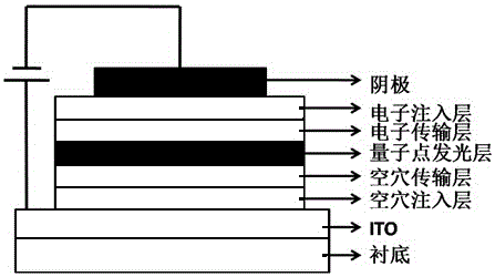
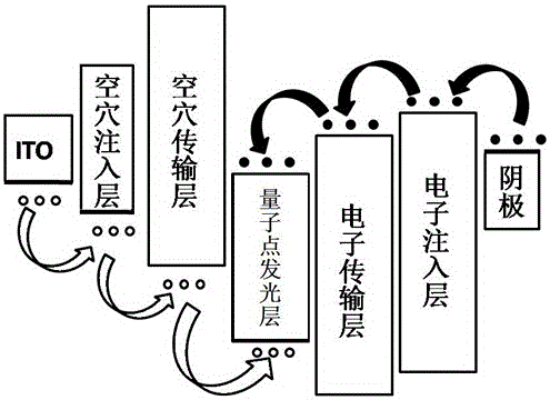
[0031] The present invention provides a method for manufacturing a hole injection layer, a hole injection layer and a QLED device. In order to make the purpose, technical solution and effect of the present invention clearer and more definite, the present invention will be further described in detail below. It should be understood that the specific embodiments described here are only used to explain the present invention, not to limit the present invention.

[0032] The invention provides a method for manufacturing a hole injection layer, which comprises the steps of:

[0033] A, the ITO substrate substrate is cleaned and then dried;

[0034] B. Surface treatment of the ITO substrate substrate;

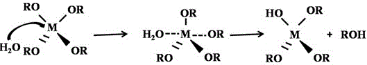
[0035] C. Attaching the transition metal oxide to the surface of the ITO base substrate, as the hole injection layer of the QLED device, the transition metal oxide is attached to the surface of the ITO base substrate by a sol-gel method.

[0036] Through the method of the present inv...


PUM

PropertyMeasurementUnit
thicknessaaaaaaaaaa
electron work functionaaaaaaaaaa

Abstract

The invention discloses a hole injection layer manufacturing method, a hole injection layer and a QLED device. The method comprises the steps of A, cleaning an ITO substrate base plate, and then drying the ITO substrate base plate; B, carrying out surface treatment on the ITO substrate base plate; and C, attaching transition metal oxides to the surface of the ITO substrate base plate so as to act as a hole injection layer of the QLED device, wherein the transition metal oxides are attached to the surface of the ITO substrate base plate through a sol-gel method. According to the invention, the transition metal oxides, which mainly comprise molybdenum oxide, vanadium oxide, tungsten oxide and the like, are adopted to act as hole injection layer materials of the QLED device so as to adjust a work function of the ITO substrate, so that the work function of the hole injection layer materials of the QLED device is enabled to be effectively adjusted in a large range, and red, green and blue quantum dots are facilitated to be able to find hole injection layer materials with good energy level matching according to the positions of valence bands, thereby effectively reducing the injection barrier of holes, and improving the luminous efficiency of the device.

Description

technical field [0001] The invention relates to the field of QLED devices, in particular to a method for manufacturing a hole injection layer, a hole injection layer and a QLED device. Background technique [0002] At present, the mainstream flat panel display in the market is realized by liquid crystal molecules. In liquid crystal display (LCD), since the liquid crystal molecules themselves cannot emit light, the participation of the backlight source is required to achieve high-quality display. However, with the introduction of the backlight source, the energy consumption problem of the LCD becomes more prominent. From the perspective of energy saving and emission reduction, the LCD is not a very ideal display technology. With the development of science and technology, organic light-emitting diodes (OLEDs) have gradually come into people's sight as a new display technology. Compared with LCDs, OLED devices are active light-emitting devices and do not require additional back...

Claims


Application Information

Patent Timeline
Patent Type & Authority Applications(China)
IPC IPC(8): H01L51/00H01L51/50
CPCH10K71/00H10K50/17H10K2102/00
Inventor 肖标付东谢相伟高卓
Owner TCL CORPORATION
Why Eureka
Try Eureka