

Amplification module suitable for class F or inverse class F power amplifier
A technology of power amplifier and amplifying module, applied in communication technology, microelectronics and semiconductor fields, can solve the problems of difficult design, long distance of transistors, and large space for harmonic matching network.
- Summary
- Abstract
- Description
- Claims
- Application Information
AI Technical Summary
Problems solved by technology
Method used
Image

Examples
Embodiment 1
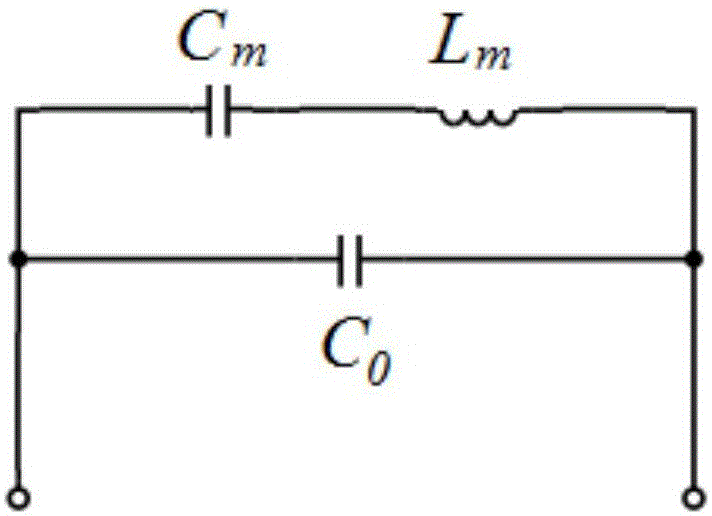
[0036] The embodiment of the invention discloses an amplifying module suitable for class F or inverse class F power amplifiers. The above-mentioned amplifying module includes a transistor, a resonator module, a base, a signal input terminal and a signal output terminal for realizing the harmonic matching required by an F-class or an inverse F-class power amplifier; the transistor includes a transistor input terminal, a transistor output terminal and a transistor ground end; the transistor and the resonator module are set on the base; the resonator module is set between the transistor output end and the signal output end; the resonator module includes a parallel resonator group and a series resonator group;
[0037] The parallel resonator group includes a first resonant module and a second resonant module connected in parallel between the output terminal of the transistor and the ground terminal of the transistor;
[0038] The series resonator group includes a third resonant mo...
Embodiment 2
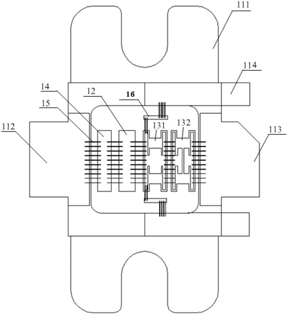
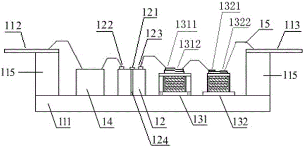
[0046] The embodiment of the present invention discloses a specific amplifying module suitable for Class F or inverse Class F power amplifiers, such as figure 2 and image 3 shown. in figure 2 is the top view of the amplification module, image 3 is a cross-sectional view of the amplifying module.
[0047] Compared with the previous embodiment, the amplifying module in this embodiment may further include a package shell, a bonding wire 15 , a 1 / 4 wavelength microstrip line 16 and an internal matching capacitor 14 . Wherein, the packaging package includes a package base 111 , a package input terminal 112 , a package output terminal 113 and a DC bias terminal 114 . Wherein, the shell base 111 is the base of the amplification module, the shell input end 112 is the signal input end of the amplification module, and the shell output end 113 is the signal output end of the amplification module; between the shell input end 112 and the shell base 111 1. Both the output terminal ...
Embodiment 3
[0061] Another modification of the amplifying module suitable for Class F or inverse Class F power amplifiers provided by the embodiments of the present invention is that the amplifying module does not need to be packaged, and the base of the amplifying module can be directly embedded on the heat sink, and then the transistor The gate of the transistor is electrically connected to the fundamental wave input matching network, the drain of the transistor is electrically connected to the fundamental wave output matching network, and the DC bias end of the drain is directly electrically connected to the DC bias end of the circuit, by This saves the package envelope.
PUM
 Abstract
Description
Claims
Application Information