Low-temperature polysilicon array substrate and manufacturing method thereof
A low-temperature polysilicon and array substrate technology, which is applied in the manufacture of semiconductor/solid-state devices, instruments, semiconductor devices, etc., can solve problems affecting the quality of LTPS array substrates, damage to the gate insulation film, and high energy consumption, etc., to reduce peeling Difficulty, reduced energy, and reduced curing effects
- Summary
- Abstract
- Description
- Claims
- Application Information
AI Technical Summary
Problems solved by technology
Method used
Image


Examples
Embodiment 1
[0058] see figure 1 , which is a schematic flow chart showing the basic flow of the manufacturing method of the low-temperature polysilicon array substrate in the embodiment of the present invention. In this embodiment, the PMOS type thin film transistor and the NMOS type thin film transistor will be prepared
[0059] In step S101 , a PMOS thin film transistor region and an NMOS thin film transistor region are formed on a glass substrate.
[0060] Such as Figure 2A As shown, this step specifically includes:
[0061] (1) Deposit a light-shielding layer on the glass substrate 100, and perform etching to form a light-shielding layer pattern 200;
[0062] (2) sequentially forming a buffer layer 300 and an amorphous silicon layer on the light-shielding layer pattern 200;
[0063](3) An amorphous silicon layer is deposited, and crystallization and etching are performed on the amorphous silicon layer to form the PMOS thin film transistor region 400A and the NMOS thin film transi...
Embodiment 2
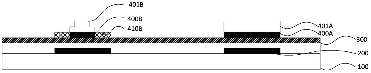
[0092] image 3 It is a block diagram of the low-temperature polysilicon array substrate in Embodiment 2 of the present invention. The low temperature polysilicon array substrate includes: a glass substrate 100 , a light-shielding layer pattern 200 , a buffer layer 300 , a polysilicon layer, and a gate insulating layer 500 .
[0093] The light-shielding layer patterns 200 , including the P-type light-shielding layer and the N-type light-shielding layer, are all deposited on the glass substrate 100 .
[0094] The buffer layer 300 is deposited on the light-shielding layer pattern 200 .
[0095] A polysilicon layer deposited on the buffer layer 300, comprising:
[0096] The PMOS thin film transistor region 400A, the boron heavily doped region 410A formed of high concentration boron in the channel formed around the PMOS thin film transistor region 400A; and
[0097] The NMOS thin film transistor region 400B, the low doped region 420B formed of low concentration phosphorus, and ...
PUM
 Abstract
Description
Claims
Application Information
PatSnap Eureka turns technology decisions into work you can execute. Powered by our Innovation Knowledge Graph, it runs expert workflows across engineering, life sciences, materials and intellectual property. Get your review-ready output in minutes.


