Directional interconnection method for Cu6Sn5-base single-crystal lead-free solder joints for high-temperature packaging

A lead-free solder joint and single crystal technology, applied in the field of materials, can solve problems that are difficult to achieve

Inactive Publication Date: 2015-12-23
HARBIN INST OF TECH SHENZHEN GRADUATE SCHOOL
View PDF6 Cites 15 Cited by
  • Summary
  • Abstract
  • Description
  • Claims
  • Application Information

AI Technical Summary

Problems solved by technology

Although there are reports in the literature that the wetting reaction between Sn-based lead-free solder and (111) single crystal Cu pads can be epitaxially formed with a large area of ​​Cu 6 sn 5 (11-20) is a multi-grain interface

Method used


Image

  • Directional interconnection method for Cu6Sn5-base single-crystal lead-free solder joints for high-temperature packaging
  • Directional interconnection method for Cu6Sn5-base single-crystal lead-free solder joints for high-temperature packaging
  • Directional interconnection method for Cu6Sn5-base single-crystal lead-free solder joints for high-temperature packaging

Examples


Embodiment 1

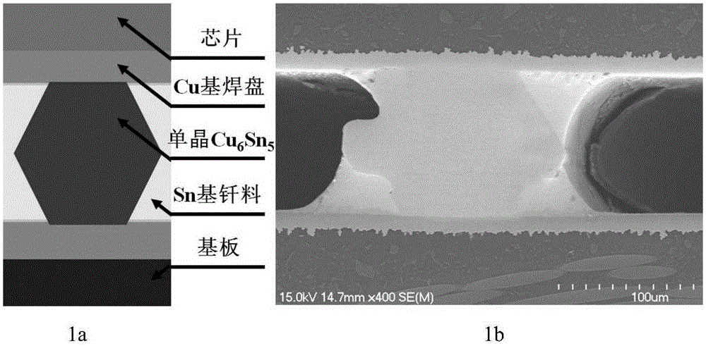
[0101] Embodiment 1 prepares Cu with a diameter of 100 μm 6 sn 5 base single crystal interconnect solder joints

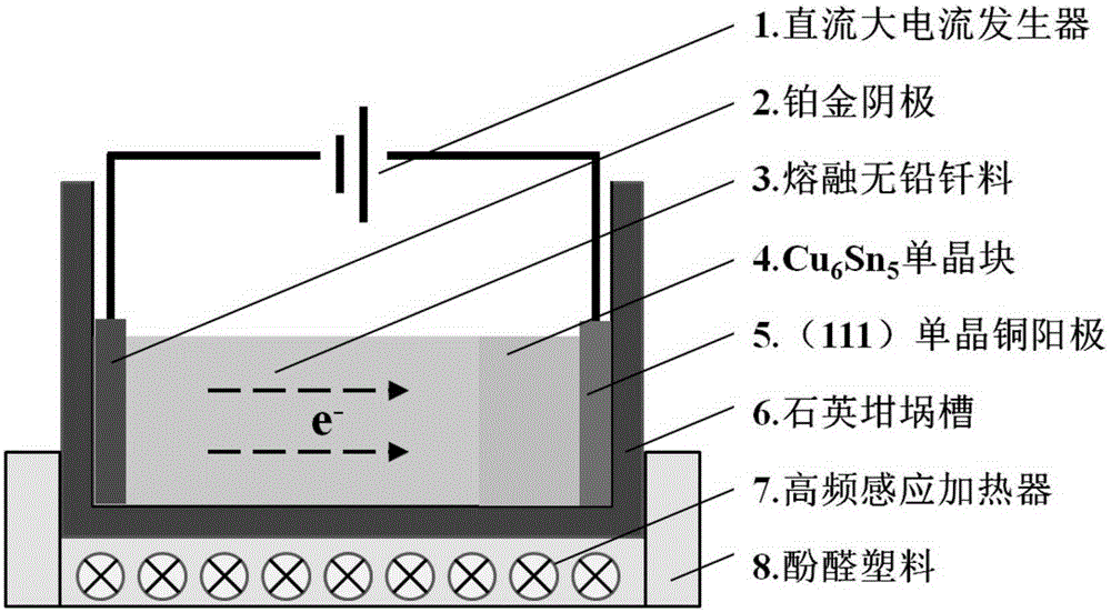
[0102] 10×10×20mm 3 Platinum cathode with 10 x 10 x 20mm 3 The (111) single crystal Cu anode is put into 100×100×30mm 3 In the quartz crucible tank, the distance between the two stages is 100mm. The two poles are respectively connected to the DC high current generator with the copper wire covered with double-layer insulating nylon to form a conductive loop. Put 0.7kg of pure Sn solder into the crucible tank, turn on the high-frequency induction heating device, wherein the heating tube is 3cm away from the bottom of the crucible tank, and the induction heating frequency is 500KHz, and continue heating to completely melt the solder. At this time, the temperature of the molten solder is about 250°C, and the volume of the solder is about 100cm 3 , exactly 1 / 3 of the volume of the crucible can be filled. open N 2 Gas protection device to prevent oxidation of mol...

Embodiment 2

[0106] Embodiment 2 prepares Cu with a diameter of 50 μm 6 sn 5 base single crystal interconnect solder joints

[0107] 10×10×20mm 3 Platinum cathode with 10 x 10 x 20mm 3 The (111) single crystal Cu anode is put into 100×100×30mm 3 In the quartz crucible tank, the distance between the two stages is 50mm. The two poles are respectively connected to the DC high current generator with the copper wire covered with double-layer insulating nylon to form a conductive loop. Put 0.7kg of pure Sn solder into the crucible tank, turn on the high-frequency induction heating device, wherein the heating tube is 4cm away from the bottom of the crucible tank, and the induction heating frequency is 750KHz, and continue heating to completely melt the solder. At this time, the temperature of the molten solder is about 265°C, and the volume of the solder is about 100cm 3 , exactly 1 / 3 of the volume of the crucible can be filled. open N 2 Gas protection device to prevent oxidation of molte...

Embodiment 3

[0111] Example 3 Preparation of Cu with a diameter of 20 μm 6 sn 5 base single crystal interconnect solder joints

[0112] 10×10×20mm 3 Platinum cathode with 10 x 10 x 20mm 3 The (111) single crystal Cu anode is put into 100×100×30mm 3 In the quartz crucible tank, the distance between the two stages is 150mm. The two poles are respectively connected to the DC high current generator with the copper wire covered with double-layer insulating nylon to form a conductive loop. Put 0.7kg of pure Sn solder into the crucible tank, turn on the high-frequency induction heating device, wherein the heating tube is 5cm away from the bottom of the crucible tank, and the induction heating frequency is 1000KHz, and continue heating to completely melt the solder. At this time, the temperature of the molten solder is about 280°C, and the volume of the solder is about 100cm 3 , exactly 1 / 3 of the volume of the crucible can be filled. open N 2 Gas protection device to prevent oxidation of ...


PUM

PropertyMeasurementUnit
Thicknessaaaaaaaaaa
Elastic modulusaaaaaaaaaa

Abstract

The invention belongs to the technical field of materials, and provides a directional interconnection method for Cu6Sn5-base single-crystal lead-free solder joints for high-temperature packaging. The method comprises the steps of firstly, preparation of a Cu6Sn5-base single-crystal block body, secondly, cutting of the Cu6Sn5-base single-crystal block body, thirdly, surface pretreatment of a Cu-base welding disc, and fourthly, interconnection of Cu6Sn5-base single-crystal welding blocks. The elasticity modulus of the Cu6Sn5-base single-crystal lead-free interconnected solder joints prepared with the method is 235% of that of common Sn-base brazing filler metal, the conductivity of the Cu6Sn5-base single-crystal lead-free interconnected solder joints is 52.4% that of the Sn-base brazing filler metal, and the heat conductivity of the Cu6Sn5-base single-crystal lead-free interconnected solder joints is 57.8% that of the Sn-base brazing filler metal. The method has the beneficial effects of being low in cost, resistant to high temperature, high in reliability of interconnection of the solder joints and a Cu-base welding disc, high in creep-resistance, and capable of being used for a long time under the severe condition. The method has the beneficial effects of being simple in working principle, low in cost, rapid in single-crystal preparation and high in quality.

Description

technical field [0001] The invention belongs to the technical field of materials, in particular to a method for directional interconnection of Cu6Sn5-based single-crystal lead-free solder joints for high-temperature packaging. Background technique: [0002] Tin-lead interconnection solder is cheap and has excellent performance, and has occupied the dominant position of interconnection materials for microelectronic packaging for a long time. However, with the enhancement of people's awareness of environmental protection and the increasing concern for their own health, the process of lead-free interconnect materials has become urgent. According to the requirements of the European Environmental Protection Directive "RoHs1", electronic products need to be lead-free from July 1, 2006; This is mainly because the industry has not yet found a lead-free solder with performance comparable to that of high-lead solder alloys (such as Sn-95Pb and Sn-90Pb) and meeting the needs of high-t...

Claims


Application Information

Patent Timeline
IPC IPC(8): B23K1/00B23K1/20B23K1/19B23K35/26H01L21/60B23K101/36
CPCB23K1/0016B23K1/19B23K1/203B23K35/262B23K2101/36H01L24/19
Inventor 李明雨张志昊操慧珺
Owner HARBIN INST OF TECH SHENZHEN GRADUATE SCHOOL
Why Eureka
Try Eureka