Manufacturing method of ring-fence non-junction nanowire transistor

A nanowire and transistor technology, applied in the micro-nano field, can solve the problems of complex transistor fabrication process and process incompatibility, and achieve the effect of improving current driving capability and suppressing mobility degradation.

Inactive Publication Date: 2015-12-23
INST OF SEMICONDUCTORS - CHINESE ACAD OF SCI
View PDF2 Cites 3 Cited by
  • Summary
  • Abstract
  • Description
  • Claims
  • Application Information

AI Technical Summary

Problems solved by technology

However, the fabrication process of vertically-structured nanowires is complex and incompatible with the silicon planar process, and it is very important to obtain laterally grown III-V nanowires

Method used


Image

  • Manufacturing method of ring-fence non-junction nanowire transistor
  • Manufacturing method of ring-fence non-junction nanowire transistor
  • Manufacturing method of ring-fence non-junction nanowire transistor

Examples


Embodiment Construction

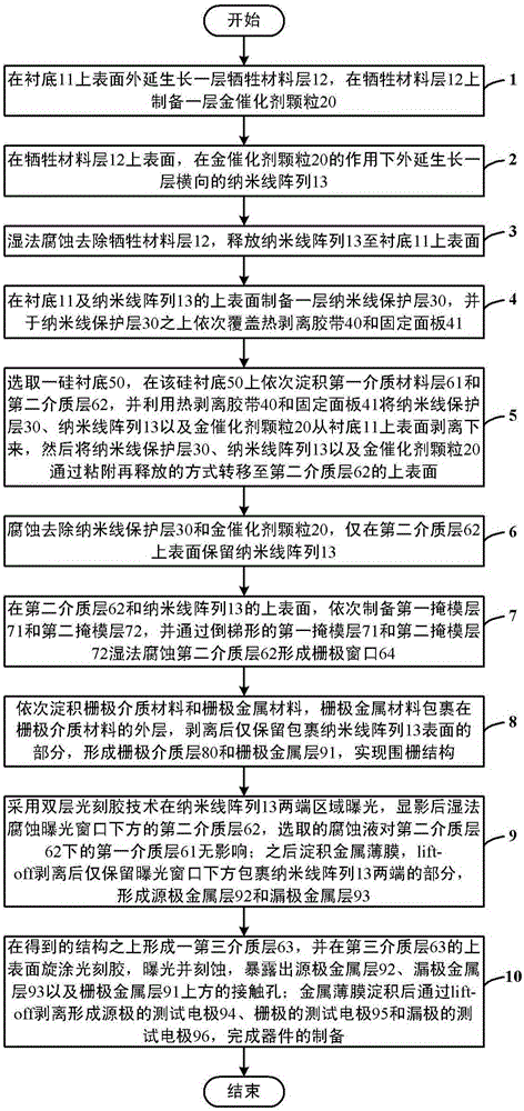
[0025] In order to make the object, technical solution and advantages of the present invention clearer, the present invention will be described in further detail below in conjunction with specific embodiments and with reference to the accompanying drawings.

[0026] The preparation method of the gate-enclosed junction-free nanowire transistor provided by the present invention adopts MOCVD to epitaxially grow doped nanowire arrays on III-V materials, and transfers the nanowires by thermally peeling tape and fixing the panel, on the silicon substrate Fabricate a junctionless nanowire transistor with a gate-enclosed structure on the bottom.

[0027] see Figure 1 to Figure 11 As shown, the present invention provides a method for preparing a gate-enclosed junctionless nanowire transistor, the method comprising:

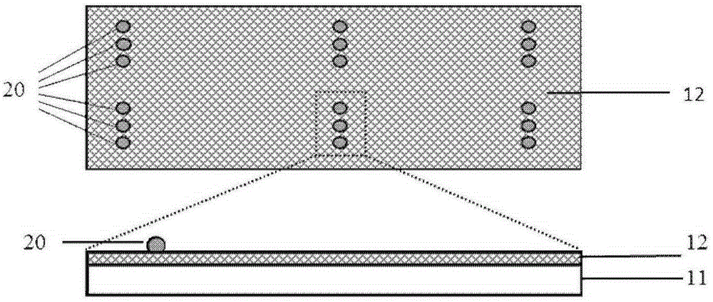
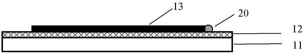
[0028] Step 1: First, epitaxially grow a layer of sacrificial material layer 12 on the upper surface of the substrate 11, and then, on the sacrificial material layer 12,...


PUM

PropertyMeasurementUnit
thicknessaaaaaaaaaa
diameteraaaaaaaaaa
thicknessaaaaaaaaaa

Abstract

The invention relates to a manufacturing method of a transistor and especially relates to a manufacturing method of a ring-fence non-junction nanowire transistor. MOCVD is used to epitaxially grow a doped nanowire array on an III-V family material. Through a thermal peeling adhesive tape and a fixing panel, the nanowire is transferred. A non-junction nanowire transistor with a ring-fence structure is manufactured on a silicon-based substrate. By using the manufacturing method of the ring-fence non-junction nanowire transistor provided in the invention, compatibility of an III-V family material nanowire and a plane silicon technology can be realized; simultaneously, mobility degeneration is effectively restrained and a current driving capability of the transistor is increased.

Description

technical field [0001] The invention relates to the field of micro-nano technology, in particular to a method for preparing a gate-enclosed junction-free nanowire transistor. Background technique [0002] Silicon-based semiconductors have achieved great success in low-cost large-scale integrated circuits, but with the substantial increase in the integration and operating speed of microelectronic devices, it has brought about a substantial increase in device power consumption, and Moore's Law is facing bottlenecks such as failure. III-V group materials not only have extremely outstanding photoelectric properties, but also have obvious advantages in electron mobility, and have been widely used in ultra-high-speed microelectronic devices and optoelectronic devices. Problems such as high cost restrict its further development. Based on silicon-based III-V materials with high electron mobility microelectronic integrated devices, it is possible to realize the complementary advanta...

Claims


Application Information

Patent Timeline
Patent Type & Authority Applications(China)
IPC IPC(8): H01L29/66H01L29/06H01L29/423H01L21/683B82Y40/00
CPCH01L29/66522B82Y40/00H01L21/6836H01L29/0673H01L29/4236H01L29/66568H01L2221/68386
Inventor 马刘红韩伟华付英春洪文婷吕奇峰杨富华
Owner INST OF SEMICONDUCTORS - CHINESE ACAD OF SCI
Why Eureka
Try Eureka