PCB manufacturing method and PCB

A PCB board and manufacturing method technology, which is applied in the manufacture of printed circuits, the formation of electrical connection of printed components, and the electrical connection of printed components, etc. The problem of unstable electrical connection between the pin and the internal copper layer of the non-plug hole can improve the accuracy of judgment, improve product reliability, and increase the area.

Inactive Publication Date: 2015-12-30
ZHUHAI FOUNDER TECH HI DENSITY ELECTRONICS +1
View PDF7 Cites 9 Cited by
  • Summary
  • Abstract
  • Description
  • Claims
  • Application Information

AI Technical Summary

Problems solved by technology

[0014] Therefore, the purpose of the present invention is to overcome that the manufacturing method of the PCB board in the prior art does not protect the non-plugging hole, the resin ink is easy to enter the inside of the non-plugging hole, and causes the detection probe and the inner copper layer of the non-plugging hole The electrical connection between them is unstable, so as to seriously affect the technical defects of the functional problems such as the electrical performance of the board during the on-off test of the PCB board, so as to provide a method that can prevent the resin ink from entering the non-plugging hole without affecting the detection The electrical connection between the probe and the inner copper layer of the non-plugged hole will not affect the functional problems such as the electrical performance of the board during the on-off test of the PCB board. The distance between the plugged hole and the non-plugged hole is too close The production method of the PCB board

Method used


Image

  • PCB manufacturing method and PCB
  • PCB manufacturing method and PCB

Examples


Embodiment 1

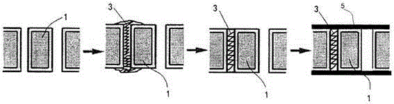
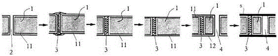
[0047] The present embodiment provides a kind of manufacturing method of PCB board, such as figure 2 shown, including the following steps:

[0048] 1) Take the substrate 1, and drill the plug hole 2 on the substrate 1;

[0049] 2) Perform the first electroplating on the substrate 1, so as to plate the first copper layer 11 on the surface of the substrate 1, and plate copper on the inner wall of the plug hole 2;

[0050] 3) Use an aluminum sheet with a through hole, then fix the aluminum sheet on the substrate 1, and make the through hole correspond to the plug hole 2, then place the resin 3 on the aluminum sheet, use a scraper on the aluminum sheet with a certain pressure and The speed is scraped back and forth, so that the resin 3 on the aluminum sheet is filled into the plug hole 2 until the resin 3 protrudes from the orifice of the plug hole 2; during this process, the viscosity of the resin 3 is controlled to 400psi, and the blade The pressure is 4Kg / cm 2 , the speed i...

Embodiment 2

[0065] This embodiment provides a method for making a PCB board, which is an improvement on the basis of Embodiment 1, and the difference is that it includes the following steps:

[0066] In the above step 4), the above-mentioned first copper layer 11 is subjected to material reduction treatment, and the part of the resin 3 protruding from the above-mentioned first copper layer 11 due to the material reduction treatment is subjected to material reduction treatment again, so that the resin 3 protrudes The surface of the opening of the plug hole 2 is again flush with the surface of the first copper layer 11 in height.

[0067] The advantage of the manufacturing method of the PCB board provided in this embodiment is that since the manufacturing method of the PCB board provided in Embodiment 1 needs to perform copper plating on the surface of the substrate 1 twice, the first copper layer 11 is plated in step 4). The material reduction treatment can avoid plating an excessively thi...

Embodiment 3

[0070] This embodiment provides a PCB board, which is manufactured by the manufacturing method described in Embodiment 1 or Embodiment 2.

[0071] The PCB board provided by this embodiment is made by using a specific manufacturing method, so it has all the advantages brought by the above-mentioned specific manufacturing method at the same time.


PUM


Abstract

The invention provides a PCB manufacturing method and a PCB. The method comprises steps that, a substrate is drilled to form a plugging hole; a first copper layer is plated on a surface of the substrate, and copper plating on an inner wall of the plugging hole is carried out; the plugging hole is filled by employing resin till the resin projects out of the plugging hole port; material decrease processing on the resin projected out of the port is carried out to make the resin project out of the surface of the port and be level with the surface of the first copper layer; the substrate is drilled to form a non-plugging hole; a second copper layer is plated on the first copper layer, and copper plating on the inner wall of the non-plugging hole is carried out; a substrate graph is shifted; the substrate is etched to form a conductive line. The PCB is manufactured through the PCB manufacturing method, the non-plugging hole quite near the plugging hole is quite clean internally, when on-off tests on the PCB are carried out, after the non-plugging hole is detected by a probe, the probe can tightly contact with the conductive copper layer of the hole wall of the non-plugging hole to realize conduction, and thereby efficiency for determining functions of the PCB can be greatly improved.

Description

technical field [0001] The invention relates to a method for manufacturing a PCB board and the PCB board, belonging to the technical field of PCB board manufacturing technology. Background technique [0002] With the rapid development of electronic products in modern society, PCB boards are becoming more and more multi-functional and highly integrated. VIP hole (in order to make the wiring space between layers wider and the degree of freedom greater, the current structural design is to directly set the via hole or micro blind hole in the pad, this via hole or micro blind hole It is called VIP hole—Viainpad, that is, the hole in the plate.) The distance between the hole and the hole is getting closer and closer, and when wave soldering is performed on the pad with the VIP hole, it is easy to leak tin and cause tin bridge short circuit. Therefore, in the PCB board manufacturing stage, VIP holes generally need to be plugged. [0003] In the traditional technology, there are m...

Claims


Application Information

Patent Timeline
Patent Type & Authority Applications(China)
IPC IPC(8): H05K1/11H05K3/42
CPCH05K1/11H05K3/42H05K2203/025H05K2203/072
Inventor 葛春朱兴华
Owner ZHUHAI FOUNDER TECH HI DENSITY ELECTRONICS
Why Eureka
Try Eureka