Ashing method for photoresist patterns

A photoresist and ashing technology, applied in the processing of photosensitive materials, etc., can solve the problems of low ashing efficiency, wafer output, impact, ion distribution changes, etc.

Active Publication Date: 2016-01-06
SEMICON MFG INT (SHANGHAI) CORP
View PDF6 Cites 2 Cited by
  • Summary
  • Abstract
  • Description
  • Claims
  • Application Information

AI Technical Summary

Problems solved by technology

[0003] However, the ashing process in the prior art tends to affect the substrate to a certain extent when ashing the photoresist pattern, such as causing recesses on the substrate surface, which will affect the devices in the substrate and subsequent processes. steps and the performance of the device; the existing ashing process may also affect the region that has been doped with ions, for example, resulting in changes in the distribution of ions in the doped region, thereby changing the performance of

Method used


Image

  • Ashing method for photoresist patterns

Examples


Embodiment Construction

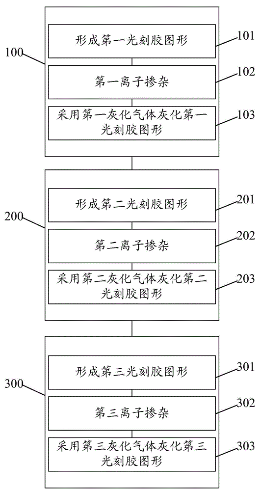
[0040] The existing ashing process easily affects the substrate when ashing the photoresist pattern. For example, the oxidation of some oxygen-containing plasmas in the existing ashing process is likely to affect the substrate of silicon material and the gates that may be contained in the substrate, and these ashing gases are also likely to cause mechanical damage to the substrate. permanent damage and form recesses in the substrate, the recesses will affect the progress of subsequent process steps and the electrical performance of the formed semiconductor device.

[0041] The existing ashing process may also affect the distribution of dopant ions in the doped regions already formed in the substrate, for example, cause the concentration of dopant ions in the doped regions to change.

[0042] Part of the dopant ions will also enter the photoresist pattern while ion doping a specific region of the substrate, so after the doping is completed, the photoresist pattern will also con...


PUM


Abstract

The invention provides an ashing method for photoresist patterns. The ashing method comprises the following steps: providing a substrate; sequentially forming photoresist patterns on the substrate at least twice; after forming the photoresist pattern each time, with the corresponding photoresist pattern as a corresponding mask, carrying out ion doping on the substrate, and doping doped ions with different contents into the corresponding photoresist pattern; and after ion doping, ashing the corresponding photoresist pattern with corresponding ashing gas containing hydrogen, wherein the ashing gases adopted for the photoresist patterns doped with the ions with different content are different in hydrogen content. The ashing method has the beneficial effects that the effects on the substrate can be reduced; the ashing rate on the photoresist patterns is also relatively high; and in addition, the control flexibility of photoresist pattern ashing is increased and the rate of ashing the photoresist patterns and the thoroughness degrees of ashing the photoresist patternscan be adjusted.

Description

technical field [0001] The invention relates to the field of semiconductor manufacturing, in particular to an ashing method of a photoresist pattern. Background technique [0002] A doping process is often required in existing semiconductor manufacturing processes. When doping, it is usually necessary to first form a photoresist pattern on the surface of the substrate to be doped to cover the region that does not need to be doped, and then dope the region exposed from the photoresist pattern. After doping, an ashing process (ashing) is generally used to ash the photoresist pattern, so as to facilitate subsequent process steps. [0003] However, the ashing process in the prior art tends to affect the substrate to a certain extent when ashing the photoresist pattern, such as causing recesses on the substrate surface, which will affect the devices in the substrate and subsequent processes. The steps and the performance of the device are affected; the existing ashing process m...

Claims


Application Information

Patent Timeline
IPC IPC(8): G03F7/36
Inventor 张海洋孟晓莹
Owner SEMICON MFG INT (SHANGHAI) CORP
Why Eureka
Try Eureka