CMOS switching circuit

A technology of switches and switching transistors, applied in the field of CMOS single-pole double-throw switches, can solve problems such as hindering CMOS technology integrated circuits, and achieve the effects of increasing isolation, reducing leakage, and reducing insertion loss

Active Publication Date: 2016-01-06
WENZHOU UNIVERSITY
View PDF5 Cites 17 Cited by
  • Summary
  • Abstract
  • Description
  • Claims
  • Application Information

AI Technical Summary

Problems solved by technology

Researchers at home and abroad have designed various CMOS transceiver switches, but there are still many difficulties in fully integrated CMOS transceiver switches that work at tens of GHz with ultra-wideband, low insertion loss, and high isolation, which hinders the application of CMOS technology in multiple applications. Frequency band, multi-branch integrated circuit

Method used


Image

  • CMOS switching circuit
  • CMOS switching circuit
  • CMOS switching circuit

Examples


Embodiment Construction

[0013] The present invention will be described in detail below in conjunction with a specific embodiment.

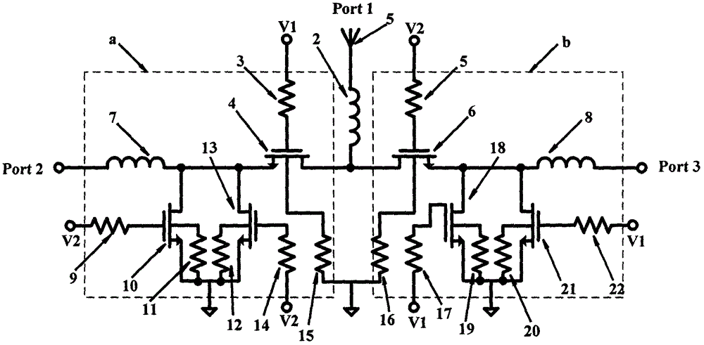
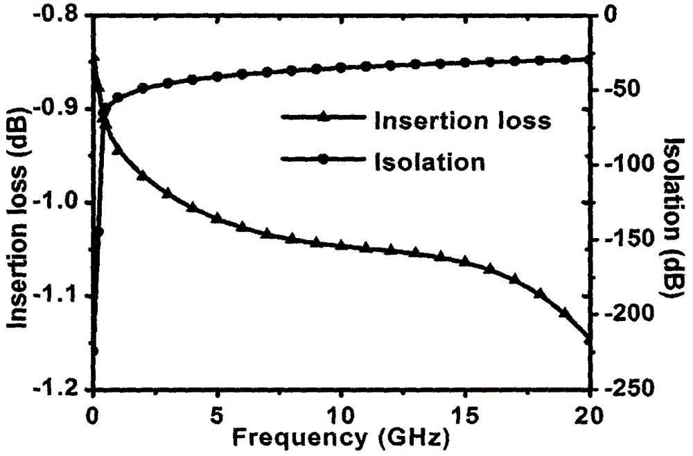
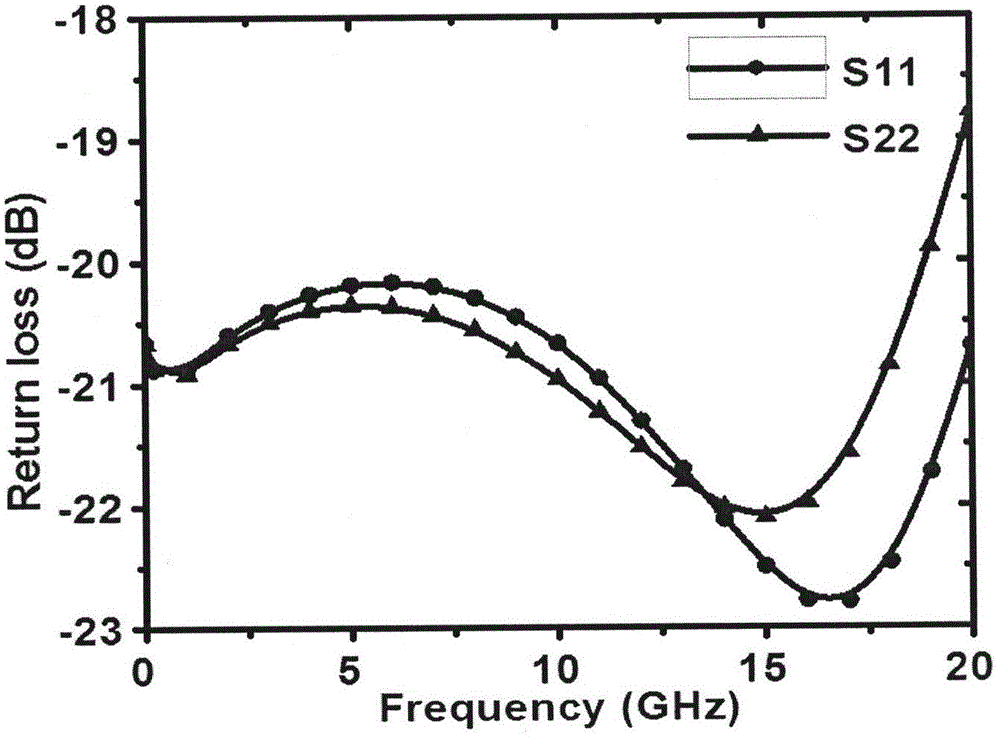
[0014] Such as figure 1 As shown, embodiments of the present invention can be used with CMOS single pole double throw (SPDT) switches. According to an embodiment of the present invention, the switch includes a receiving circuit and a transmitting circuit, which can work in the frequency band of 0-20 GHz, and meet the requirements of low insertion loss, high isolation and low input and output reflection coefficients. These points will be described below described in further detail.

[0015] According to the present invention, by figure 1 In the embodiment, the CMOS switch includes a receiving switch circuit a and a transmitting switch circuit b. The CMOS switch may include an antenna 5 for communicating with at least one of the receiving switch a and the transmitting switch b.

[0016] According to an exemplary embodiment of the present invention, the antenna 5 may be...


PUM


Abstract

The invention belongs to the technical field of integrated circuits, and specifically provides a CMOS single pole double throw transceiver switch, which has low insertion loss, a high isolation degree and a low input and output reflection coefficient. The CMOS single pole double throw transceiver switch comprises a receiving switch and a transmitting switch. The CMOS single pole double throw transceiver switch provided by the invention adopts the deep N well technology, the bodies of all the transistors are connected to the ground, and N wells are connected with a supply voltage to minimize the capacitance between the bodies and a matrix; the CMOS single pole double throw transceiver switch provided by the invention adopts the inductance matching technology to achieve impedance matching at three ports; and in the CMOS single pole double throw transceiver switch provided by the invention, the grid electrodes of all the transistors are serially connected with a substrate. The CMOS single pole double throw transceiver switch provided by the invention can effectively reduce the leakage of a low radio frequency signal, reduce the insertion loss of the switch, and can increase the isolation degree of the switch at the same time. The CMOS single pole double throw transceiver switch provided by the invention can be integrated to a system-on-chip Soc or an application-specific integrated circuit ASCI or the like under a low voltage of 1.8V and working frequency of 0-20GHz.

Description

technical field [0001] The invention belongs to the technical field of integrated circuits, in particular to a CMOS single-pole-double-throw (single-pole-double-throw, SPDT) switch with low insertion loss, high isolation, and low input-output reflection coefficient. Background technique [0002] The on-chip integrated transceiver switch is a key component of the wireless communication system. Using the on-chip transceiver switch can realize that the receiving and transmitting circuits on the chip share an antenna; if the antenna is integrated on the chip, the on-chip integrated transceiver switch will greatly save the chip area, because the antenna The area is relatively large, which can reduce the cost. Most high-performance radio frequency integrated circuit switches adopt GaAs technology, especially those switches with several GHz bandwidth and high power handling capability. Silicon-based CMOS has become an ideal choice for high-performance broadband transceiver switche...

Claims


Application Information

Patent Timeline
Patent Type & Authority Applications(China)
IPC IPC(8): H03K17/687
Inventor 刘桂翟耀宗孙力张丰温作威
Owner WENZHOU UNIVERSITY
Why Eureka
Try Eureka