

A kind of ER, YB co-doped Al2O3/AG double-layer up-conversion luminescent film and its preparation method
A technology of light-emitting film and double-layer film, applied in the fields of photoluminescence and solar cells, can solve the problems of affecting up-conversion light-emitting enhancement, etc., and achieve the effects of enhancing up-conversion light-emitting performance, good process stability and high repeatability
- Summary
- Abstract
- Description
- Claims
- Application Information
AI Technical Summary
Problems solved by technology
Method used
Image


Examples
Embodiment 1
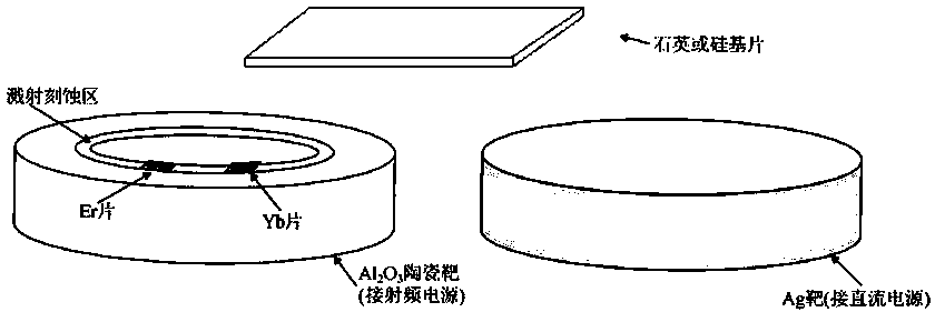
[0039] Preparation of Er﹑Yb co-doped Al 2 o 3 Thin film: Among them, Er: 0.8 mol%, Yb: 10 mol%. The substrate temperature is room temperature, the oxygen partial pressure in the sputtering gas accounts for 1.8% of the total gas pressure, the sputtering pressure is 0.8Pa, and the sputtering power density is 106 kW / m 2 , the thickness of the film is 500nm, and it is annealed in air at 1000°C for 150min.
[0040] The pump source for measuring luminescence is a 980nm semiconductor laser with a power of 2W and incident on the surface of the film at an angle of 45°.
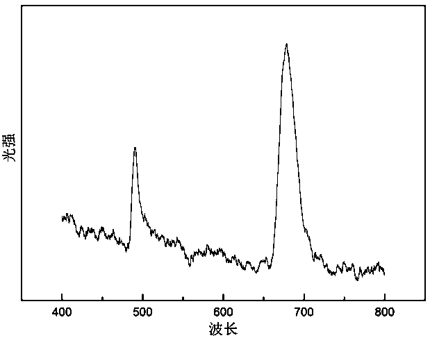
[0041] image 3 It is the upconversion luminescence spectrum of the thin film sample in Example 1 excited by the pump source.
Embodiment 2
[0043] Preparation of Er﹑Yb co-doped Al 2 o 3 / Ag double-layer film, in which, Er: 1mol%, Yb: 20mol%, Al 2 o 3 Other film preparation conditions are the same as in Example 1, and the film thickness is 500nm;
[0044] Preparation of Ag film: substrate temperature is room temperature, sputtering gas is argon, sputtering pressure is 0.6Pa, sputtering power density is 7.1kW / m 2 . Ag film thickness (a) 0 nm, (b) 14 nm.
[0045] Figure 4 is the upconversion luminescence spectrum of the thin film sample in Example 2 under the excitation of the pump source.
Embodiment 3
[0047] Preparation of Er﹑Yb co-doped Al 2 o 3 / Ag double-layer film, in which, Er: 0.5mol%, Yb: 5mol%, Al 2 o 3 Other film preparation conditions are the same as in Example 1, and the film thickness is 500nm;
[0048] Preparation of Ag film: substrate temperature is room temperature, sputtering gas is argon, sputtering pressure is 0.6Pa, sputtering power density is 5.3kW / m 2 . Ag film thickness (a) 0 nm, (b) 14 nm.
PUM
| Property | Measurement | Unit |
|---|---|---|
| thickness | aaaaa | aaaaa |
| thickness | aaaaa | aaaaa |
Abstract
Description
Claims
Application Information